LED PCB Soldering Defects: How to Find the Cause and Prevent Repeat Failures

On This Page (Table of Contents)
Most LED PCB soldering defects fall into five groups: solder bridges, incomplete or cold joints, poor wetting, tombstoning, and voids under thermal pads. A reversed LED is not a solder-joint defect, but it belongs in the same first-pass check because the symptom can look identical: one LED—or a whole series string—stays dark.
The tricky part is that the symptom rarely tells you the cause. Turning up the oven might help an under-reflowed joint. It will not fix oxidation, uneven paste deposits, or a reversed part. Classify the defect first. Then follow the evidence back to design, printing, placement, reflow, or materials.
Map LED PCB Soldering Defects Before You Guess the Cause
Here is the trap: different defects can produce the same board-level symptom.
A dark LED may have an open joint, reversed polarity, component damage, or a circuit problem. A short may come from a visible solder bridge, but that bridge may have started with stencil design, paste volume, placement offset, or unstable printing.
Voids are different again. They sit inside the solder layer, so the inspection method that finds a bridge or tombstoned part may not tell you anything about the thermal pad.
| Defect or Error | Typical Board Effect | First Area to Check | Useful Verification |
|---|---|---|---|
| Solder bridge | Short or incorrect current path | Paste print, stencil, spacing, placement | Magnified inspection or AOI |
| Incomplete or cold joint | Open, intermittent light, unstable contact | Paste, surface condition, actual reflow | Joint inspection plus process evidence |
| Poor wetting or non-wetting | Weak or incomplete connection | Finish, contamination, flux, paste, profile | Material history plus joint inspection |
| Tombstoning | One open termination | Pad, paste, thermal symmetry, placement | Print and placement evidence plus visual/AOI |
| Thermal-pad voiding | Higher thermal resistance or local hot-spot risk | Aperture, paste, via design, wetting, profile | X-ray where applicable plus thermal review |
| Wrong LED orientation | LED or series string does not light correctly | Datasheet, feeder, program, first article | Polarity inspection plus functional check |
Treat the symptom as a clue, not a root-cause conclusion. Use the table to decide where to begin.
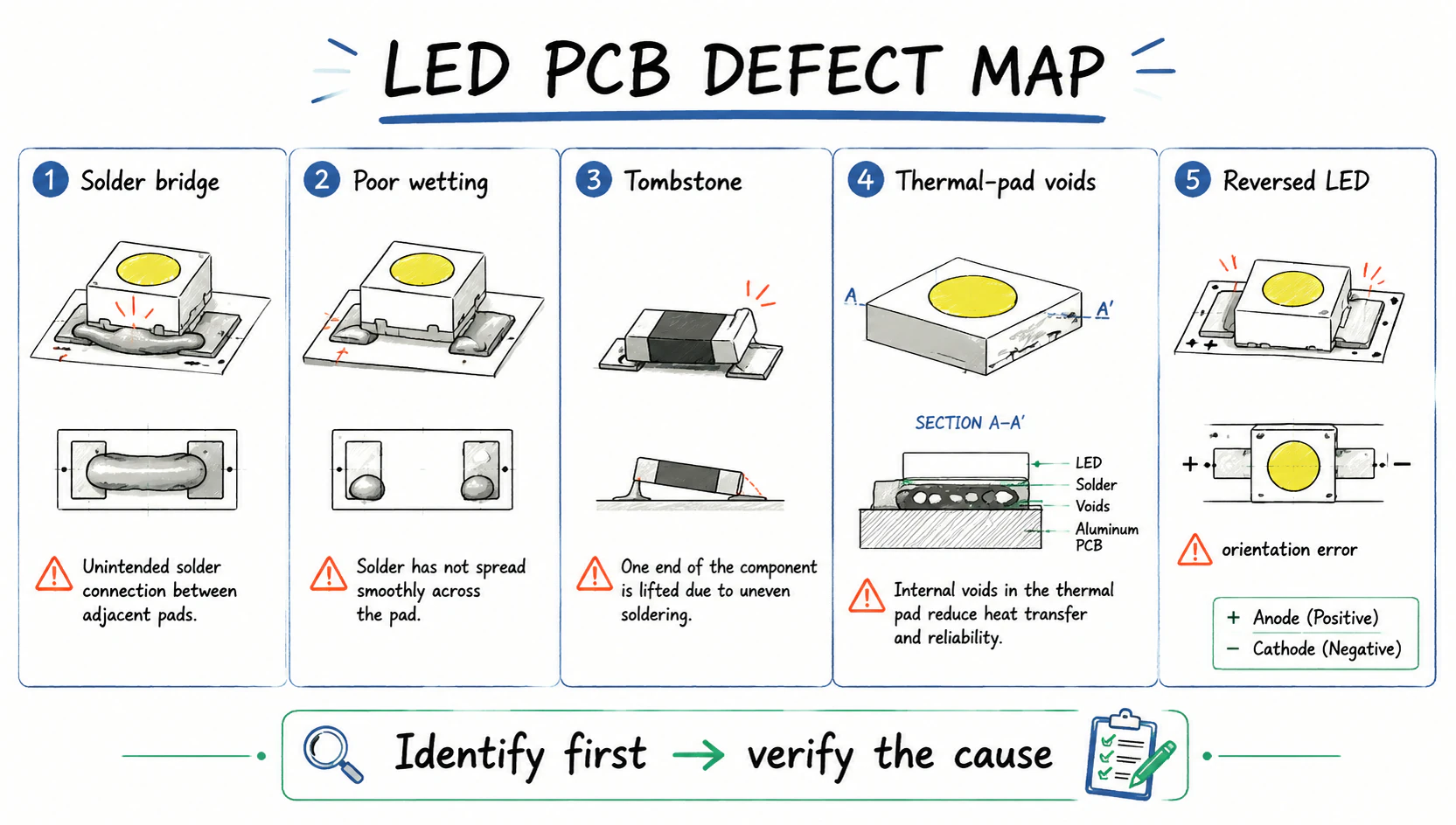 These issues can create similar board-level symptoms, so identify the physical defect before changing the process.
Solder Bridging: The Pattern Tells You Where to Look
A solder bridge is an unintended connection between adjacent pads, leads, or conductors. Finding the bridge is usually straightforward. Finding out why it formed takes a little more work.
Excess or offset paste, stencil misalignment, paste slump, tight spacing, placement offset, or unstable board support can all contribute.
The pattern gives the first clue. A bridge repeated at one designator suggests a systematic design, stencil, or program issue. Random bridges point more toward print stability, handling, or process drift. If one package family is affected, compare its aperture, nozzle, centroid, and component dimensions.
AOI can help detect visible bridges, but it does not explain why they formed. The repeat pattern often tells you more than one close-up photo.
Cold Joints and Poor Wetting: Why More Heat May Not Help
An incomplete or cold joint did not form a reliable connection. Poor wetting means the molten solder did not spread and bond correctly to the pad or component termination.
This is where troubleshooting often goes off track. The oven gets blamed first, even though oxidation, contamination, flux condition, paste handling, and surface finish can create a similar result.
Measure the Joint—not Just the Oven Recipe
An oven setpoint does not prove that the coldest joint reached the solder paste’s required reflow window.
Board and panel size, copper distribution, component mass, fixtures, and oven loading can change the local response. A joint in a thermally demanding area may receive insufficient exposure even when the machine recipe looks normal.
That does not mean the answer is always more heat. The hottest LED package must also remain inside its permitted exposure. A useful reflow check therefore compares the coldest joint with the hottest sensitive component on a representative board.
Check the Materials Before Blaming Temperature
A measured profile can look reasonable while a material or surface problem still prevents proper wetting.
Check:
- solder paste storage, warm-up, open time, and working condition
- flux activity and compatibility with the profile
- pad-finish age, storage, handling, and contamination
- oxidation or contamination on component terminations
- whether the paste, PCB finish, and LED termination were qualified together
The technical guidance from Kester and AIM Solder points to the same mix of variables: heat, flux, oxidation, and material handling.
A Dull Joint Is Not Automatically a Cold Joint
Lead-free solder can look less shiny than traditional tin-lead solder. Color or gloss alone is therefore not enough to prove a cold joint.
Evaluate the complete joint shape, evidence of wetting, electrical behavior, applicable acceptance requirement, and process history. An intermittent LED can be consistent with a connection problem, but the electrical path still needs to be verified.
If an incomplete joint appears at a high-mass area, check the actual-board profile there. If solder does not spread, review the finish history and paste condition. If the defect increases after paste sits on the stencil, compare the line timing with the paste working-life guidance.
More heat is not a substitute for paste in good condition and clean, solderable surfaces. Our guides to SMT solder paste for aluminum PCB and aluminum PCB surface finish explain those interfaces in more detail.
Tombstoning Is a Balance Problem
Tombstoning happens when one end wets or pulls before the other. The component standing upright is only the final event; the imbalance usually started earlier.
Work through four checks:
- Pad and thermal balance. Are both ends connected to similar copper areas and heat paths?
- Paste deposits. Do both pads receive comparable aperture geometry and solder volume?
- Placement. Is the component centered on the pads and paste?
- Reflow timing. Do both ends reach wetting conditions close enough together?
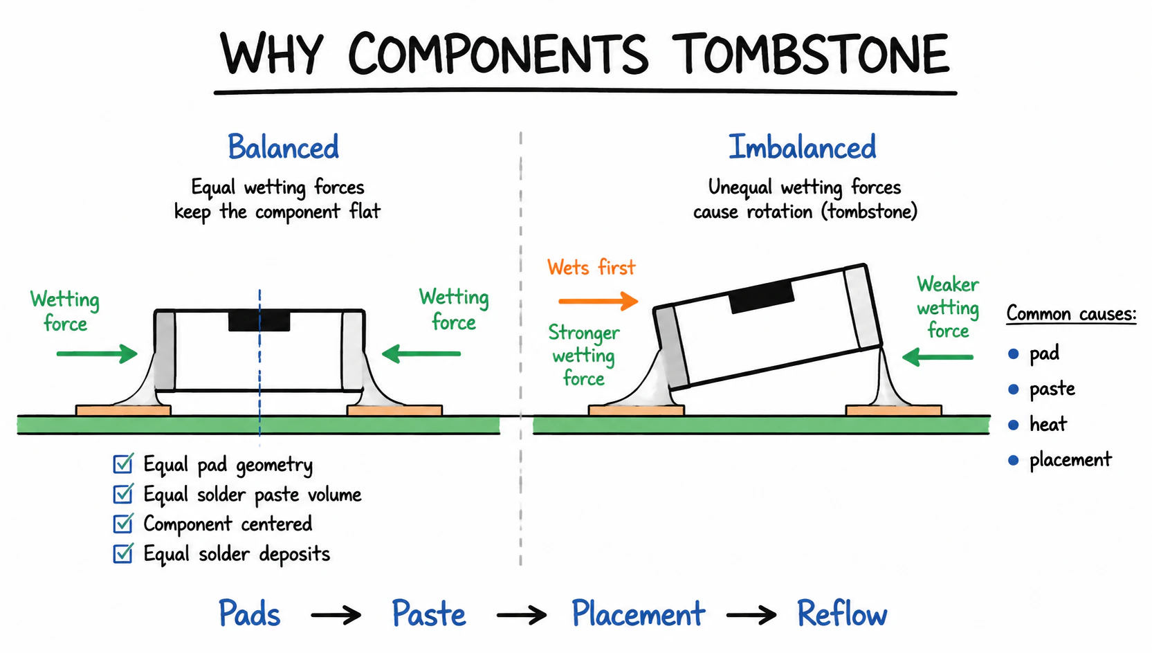 Tombstoning starts when pad, paste, placement, or thermal differences let one end wet and pull before the other.
Indium’s explanation of tombstoning describes the same underlying issue: unbalanced wetting forces. Pad geometry, thermal sinking, paste volume, placement, alloy behavior, and the profile can all influence that balance.
That gives you a sensible order of attack: pad and thermal balance first, then paste deposits, placement, and the measured reflow response. Consider paste or alloy changes only after those variables are understood.
No single stencil pattern, alloy, soak profile, or atmosphere prevents tombstoning on every LED board. Tombstoning is a balance problem, so the fix has to address the imbalance.
Thermal-Pad Voids: Percentage Alone Is Not Enough
Voids are internal gas pockets or discontinuities in the solder layer. Under an LED thermal pad, what matters is how much of the heat path they interrupt, where they sit, and whether they form one large blockage or several smaller voids.
A void percentage without package and location context is incomplete evidence.
A large central void may disrupt a critical heat-flow area differently from several smaller, distributed voids. The result also depends on package construction, solder-joint geometry, PCB thermal design, vias where applicable, and the cooling path beyond the board.
Voiding can be influenced by several interacting factors:
- flux outgassing under a large pad
- thermal-pad and stencil-aperture geometry
- paste volume and chemistry
- via design or solder wicking
- pad condition and wetting
- reflow timing
- repeated thermal exposure
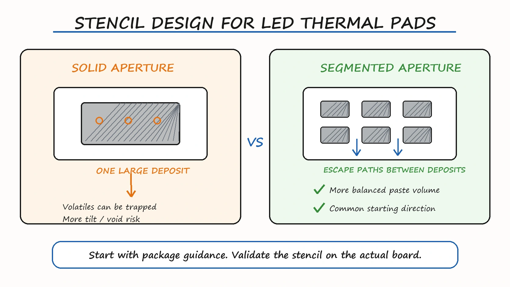 Segmented apertures can help control paste distribution and gas escape, but the final design still depends on the LED package and actual process.
Segmented or window-pane stencil apertures are a common engineering direction because they can control deposit shape and create paths for volatiles to escape. But they are not one universal design. Start with the exact LED manufacturer’s land-pattern and assembly guidance, then validate the actual print and reflow process.
X-ray may be appropriate when a hidden thermal-pad joint must be evaluated. It is not automatically required for every standard LED board, and the inspection scope should be confirmed for the project.
Instead of asking whether one percentage is acceptable in every case, confirm the package, void location and distribution, measurement method, and applicable requirement. See our guide to LED aluminum PCB heat dissipation for the wider thermal path.
A Reversed LED Can Look Like a Bad Solder Joint
This one is easy to misdiagnose. An LED can stay dark even when both solder joints are physically sound—simply because the part was placed in the wrong orientation.
Polarity marks can differ across manufacturers, package families, colors, and substitute parts. The safe reference is the datasheet for the exact manufacturer part number, not a generic diode convention or body shape.
The orientation check should cover the exact BOM part number, datasheet polarity mark, tape and feeder direction, centroid rotation, machine-vision reference, assembly drawing, and first article.
AOI can check a visible polarity mark when correctly programmed. But a wrong AOI reference can approve a consistently wrong placement, and some marks are difficult to see. A functional light test can catch some visual escapes, although another circuit fault can create the same symptom.
If a design uses several LED colors, suppliers, or substitutes, treat each part number as a separate orientation-risk item. Correct soldering cannot compensate for a reversed LED.
On Aluminum PCB, Profile the Build—not the Material Name
The metal core matters, but it does not deserve the blame for every weak joint. Paste, LED package, panel size, copper distribution, component mix, and the measured board response still need to be evaluated together.
In a normal LED MCPCB, the solder joints form on finished copper pads—not on the bare aluminum base. The metal-core stack affects heat spreading and the complete assembly’s thermal response.
Board and panel dimensions, copper distribution, component mix, fixtures, and oven loading still affect the thermal response.
Use a simple control hierarchy:
- selected solder-paste technical data
- exact LED and component limits
- thermal verification on the actual or representative build
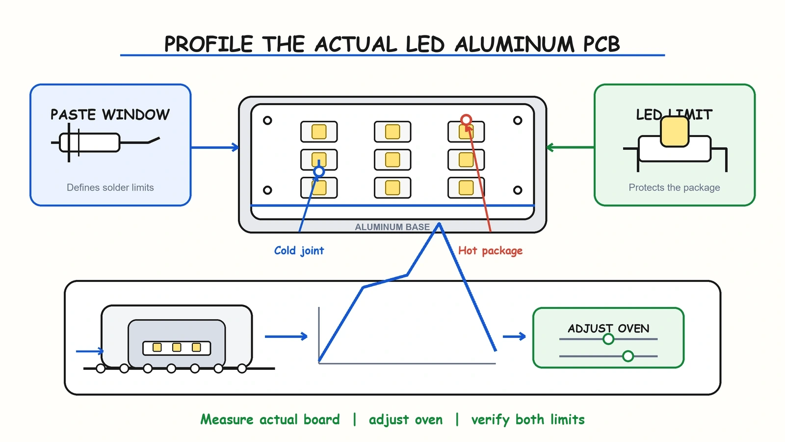 Check the actual assembly against both the solder-paste window and the LED package limit.
Do not assume every aluminum PCB needs a higher peak, longer soak, slower ramp, or simply “more heat.” A defect may still begin with stencil design, paste condition, PCB finish, placement, contamination, or component handling.
The better question is not “Did you make the aluminum profile hotter?” Ask: Was this build checked inside both the paste and LED limits? Read our reflow soldering aluminum PCB guide for the full process logic.
Prevention Has to Start Before Inspection
Final inspection is a safety net, not the first quality control. A stable process uses design, printing, placement, reflow, and verification to stop different defects at different stages.
| Control Layer | Main Defects It Helps Prevent or Catch | What Buyers Should Confirm |
|---|---|---|
| DFM and documentation | Tombstoning, bridging, polarity mismatch, thermal-pad risk | Footprint, polarity, package note, substitutions |
| Stencil and paste | Bridges, insufficient solder, tombstoning, voiding | Aperture, paste condition, print control |
| Placement | Offset parts, tombstoning sensitivity, reverse polarity | Feeder, rotation, vision, first article |
| Reflow | Incomplete reflow, poor wetting, process-related voiding | Paste/component window on actual build |
| Inspection and test | Visible defects, hidden joints, functional escapes | Included method and acceptance scope |
| Feedback and change control | Repeat failures after revisions or substitutions | Batch trend and approval triggers |
Get DFM and Documentation Right First
Defect prevention starts before the stencil or placement program is released.
Review pad geometry, spacing, thermal balance, thermal-pad design, exact LED part numbers, polarity notes, and approved substitution rules. A correct assembly program cannot fix an unsuitable footprint or an ambiguous polarity definition.
Control the Paste Deposit and Placement
Paste volume and position establish the starting condition for every solder joint.
Aperture design, stencil condition, paste handling, board support, and print alignment can influence bridging, insufficient solder, tombstoning, and voiding. Placement controls then need to confirm component position, tape direction, rotation, and the exact LED orientation.
Verify Reflow, Then Match Inspection to the Defect
Reflow should be verified on a representative build inside both paste and component limits. The inspection method should then match the defect it can actually see or measure.
Visual inspection and AOI can catch many visible bridges, tombstones, and placement errors. Hidden thermal-pad conditions may need X-ray where the package or requirement justifies it. Electrical or functional testing should be agreed according to the project.
The final layer is change control. If the board, panel, paste, LED package, supplier lot, stencil, or program changes, review whether the sample or process needs to be validated again.
For stable repeat production, catching a defect is useful. Preventing the same defect after a change is better. Our SMT production line overview explains where these controls fit in the wider assembly flow.
Give Your Assembly Partner More Than a Close-Up Photo
A close-up shows what the defect looks like. It rarely shows why it happened.
A useful report also explains where the problem occurred, how often it repeats, when it appeared, and what changed before the failure.
Include:
- board revision and order or batch identifier
- component designator and exact manufacturer part number
- inspected quantity and defect count
- whether the defect repeats at the same location, package family, or panel position
- electrical symptom: short, open, intermittent, unlit LED/string, or overheating
- when the failure appeared: after reflow, test, aging, transport, or field use
- clear full-board and close-up photos
- assembly drawing and polarity reference
- AOI, X-ray, electrical, profile, or functional evidence when available
- recent changes in finish, paste, stencil, component, supplier lot, panel, or program
Useful details are specific: D12 on panel positions 3 and 6, 8 of 500 boards inspected, the complete series string is open, or the LED supplier lot changed. This does not need to be a formal 8D report every time. It needs enough detail to compare the defect with the board, batch, materials, and process.
When preparing a new assembly, the same principle applies before production: send complete board and assembly files rather than only a Gerber. Our PCB assembly quote guide covers the BOM, pick-and-place file, assembly drawing, and other useful inputs.
Conclusion
A practical LED PCB defect investigation follows five steps:
- Classify the physical defect or orientation error.
- Map it to the likely design, print, placement, reflow, material, or inspection stage.
- Collect evidence before changing the process.
- Correct the supported cause rather than one convenient variable.
- Validate the corrected sample before releasing repeat batch production.
Two misdiagnoses are worth avoiding. A reversed LED can look like a solder failure even when the joints are sound. And an aluminum PCB can change the thermal response without being the root cause of every weak joint.
If you are preparing a single-sided aluminum LED PCB or scheduling an LED PCB SMT assembly run, send the Gerber files, BOM, pick-and-place file, exact LED datasheets, quantity, and required inspection or test notes. If you already have a defect, include clear photos, affected designators, batch information, and the failure pattern.
Lumina can first confirm whether the project fits its aluminum PCB + SMT scope before quotation and sample production.
Need a quotation?
Send Gerber files and basic specifications. We reply within 1 business day.
Ask for Quote