Automatic X-Ray Inspection (AXI): When LED Boards Actually Need It

On This Page (Table of Contents)
Automatic X-ray inspection (AXI) looks at solder joints a camera cannot see.
That's the whole job. The system sends X-rays through the assembled board and checks the solder under packages like QFNs, LED thermal pads, and BGAs.
On many single-sided LED aluminum boards, you do not need this on every panel. Visible LED and resistor joints are usually handled with paste control, reflow, AOI, and a lighting test.
X-ray starts to matter when a hidden thermal pad or a bottom-terminated package sits in the heat or power path. Even then, name those joints. "X-ray the whole board" is rarely the useful request.
Here's what this guide covers:
- What AXI is (and what it is not)
- What it can catch that AOI misses
- How AXI, AOI, and a lighting test split the work
- When LED boards actually need X-ray
- How to write it into an RFQ
One factory note up front: Lumina inspects visible work with AOI. We do not run an AXI line. This is a buying guide, not a machine we sell.
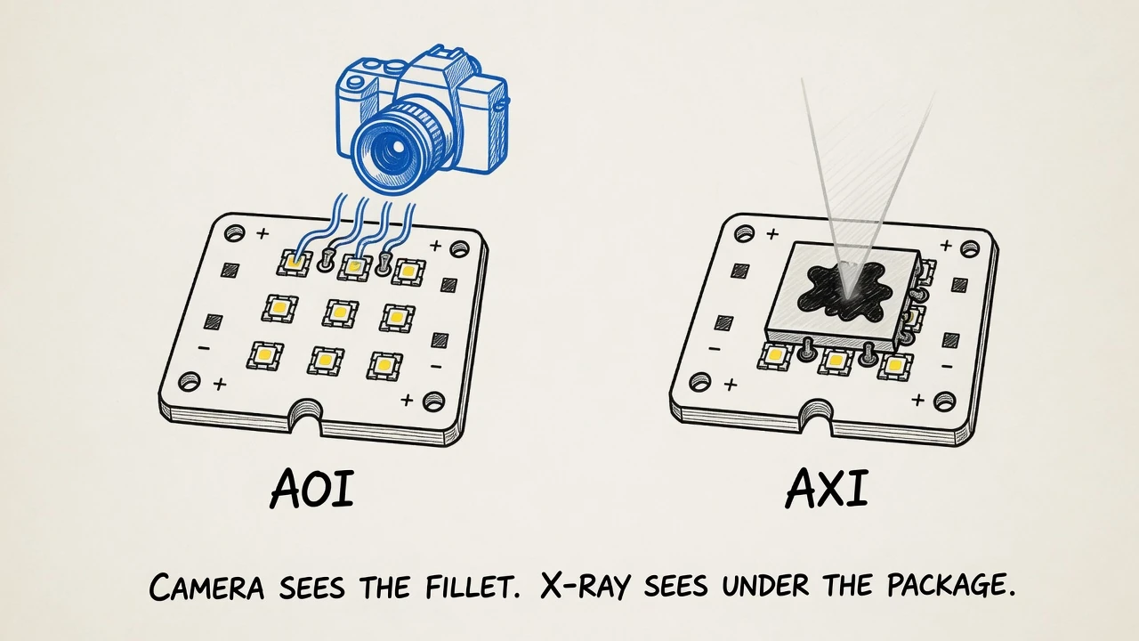 AOI looks at exposed fillets. AXI is for the solder a camera cannot see under the package.
What Is Automatic X-Ray Inspection (AXI)?
AXI is automated X-ray inspection of assembled boards. The system sends X-rays through the PCBA, then software compares the hidden solder joints against a programmed recipe.
Think of it as AOI's cousin.
AOI uses light. AXI uses X-rays. That's why AXI can look under a QFN or an LED thermal pad.
GÖPEL describes it as a non-destructive quality process for PCBAs, especially joints under BGAs and QFNs. A 2018 NDT review says the same thing in one line: AXI works like AOI, except it uses X-rays instead of visible light.
Three things AXI is not:
- It is not an electrical test.
- It is not proof the joint will last in the field.
- It is not an IPC rule that every PCBA must follow.
IPC-A-610 and J-STD-001 tell you how an assembly should look and how it should be soldered. The public pages for those documents do not say every board needs AXI.
IPC's 2024 J-revision note added graphics for bubbles in X-ray images. That's a documentation update, not a mandate to X-ray every LED lamp board.
2D vs 3D
Drawings sometimes name 2D or 3D. Here's the difference.
2D is one picture through the stack. It's fast when the joint is sitting by itself.
3D / CT builds slices from several angles. Use it when vias, copper pour, or other metal sit on top of the joint you need to judge.
GÖPEL's LED inspection note shows a via-under-pad case where a 2D void number is hard to trust.
So don't order 3D because it sounds more advanced. Order the view that can isolate the characteristic you named. If your drawing already says 2D or 3D, keep that wording attached to specific reference designators.
What Can AXI Find That AOI Cannot?
AOI stops where light stops. AXI is for solder under a package body, or inside a plated hole.
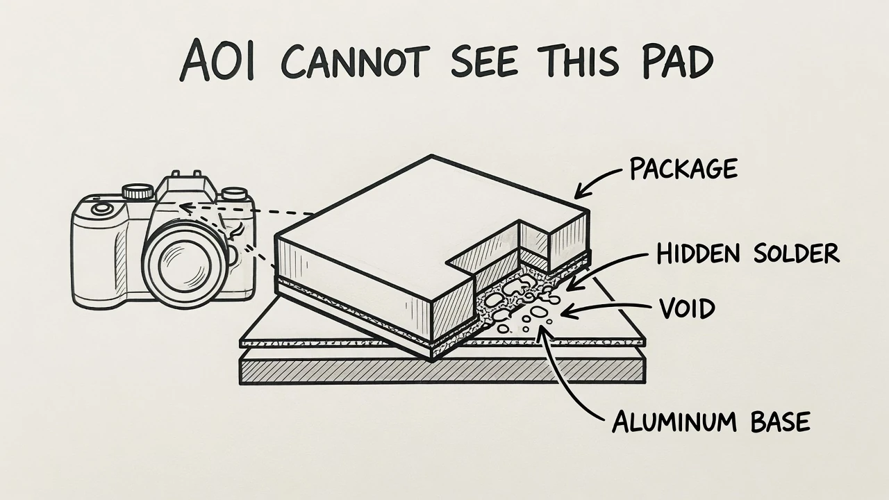 The thermal pad sits under the package. AOI never gets a line of sight to that solder.
Here's the simple split:
| Hidden condition | Why AOI misses it | What X-ray can add | Watch-out |
|---|---|---|---|
| QFN / BTC thermal-pad voiding | The pad is under the package | Soldered area and void distribution | Vias can bias a 2D number |
| BGA voids and bridges | The joint is under the package | Density gaps and ball-to-ball shorts | The accept limit is product-specific |
| Missing or thin hidden solder | There is no visible fillet | Low-density or missing solder | Subtle non-wet opens may not show |
| Lifted or non-contact geometry | The body blocks the interface | Gross separation | Not every open is visible |
| Head-in-pillow indication | The interface is hidden | Suspicious ball/paste geometry | An indication, not a confirmed diagnosis |
| PTH barrel fill | The surface fillet can look fine | Internal fill and pin penetration | The view has to be readable |
Nordson's AXI applications list covers lifted joints, insufficient solder, voiding, head-in-pillow, bridges, and PTH barrel fill. Infineon's QFN assembly guide adds a limit: broken solder joints are not easily detected by X-ray.
What does that mean for buyers?
AXI can screen for hidden density and geometry problems. It cannot promise that every open, crack, or head-in-pillow defect will be caught.
And a void is a measurement, not automatically a reject. Size, location, and the rest of the thermal path still decide whether it matters.
Visible LED soldering defects such as bridges or incomplete fillets often show up under AOI. Hidden-pad voids are the ones a camera will miss.
AXI vs AOI vs Lighting Test
These three methods answer three different questions.
AOI: is the part there, facing the right way, with a visible fillet that looks right?
AXI: is there solder under a package a camera cannot see?
Lighting test: does the board actually light?
None of them replaces the others.
Solder-paste inspection (SPI) sits one step earlier. It checks paste volume and registration before reflow, which can prevent later hidden-joint problems. SPI is a common SMT control. It is not a confirmed Lumina process.
| Method | What it inspects | Typical role on an LED aluminum board | At Lumina |
|---|---|---|---|
| AOI | Visible parts, polarity marks, exposed solder | Broad screen for LEDs and passives | Confirmed visual inspection gate |
| AXI | Hidden solder geometry | Named thermal pads, QFNs, power packages | No AXI production line |
| Lighting test | Operating behavior | Confirms the board lights | Discuss in the RFQ; do not assume a specific tester |
AXI does not read polarity marks. AOI does not see under a QFN. A lighting test can pass while a thermal pad is poorly soldered.
If you only ask "do you have AXI?", you skip the better question: which joints on this LED board are hidden?
On Lumina's SMT line, the confirmed visual gate is AOI. If a drawing also requires AXI, put that in the RFQ. Don't assume it is an in-house step.
When LED Boards Actually Need X-Ray, and When They Do Not
Most single-sided LED arrays with visible LED and passive joints do not need 100% X-ray.
That's the default. X-ray becomes a real discussion when a hidden joint is part of the heat or power path, or when you need process evidence after a change.
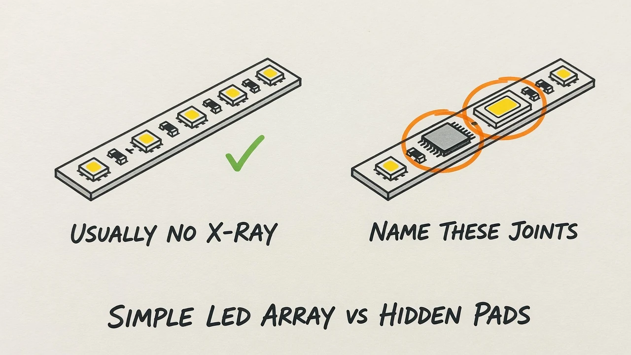 A visible LED strip usually stays on AOI and lighting test. Name the hidden pads if they are in the heat or power path.
You probably need to discuss X-ray if:
- High-power LED or CSP thermal pads carry heat into the board
- The driver or power IC is a QFN, BTC, or exposed-pad package
- You're in NPI, or you just changed stencil, paste, reflow, or via treatment
- A power or high-current through-hole needs internal fill evidence
You probably don't if:
- The board is a simple single-sided LED array with visible fillets
- AOI can see polarity and solder, and a lighting test covers function
- The request is "100% X-ray the whole panel" with no named targets
Texas Instruments' QFN/SON attachment note is useful here. It says X-ray is typically used to set process parameters and then monitor production. In most cases, 100% inspection is not performed.
Infineon's Power QFN note says the same kind of thing: sample X-ray during setup and on production samples is more common than X-raying the whole run.
Those are component-maker practices, not a rule that every LED lamp must follow. They also cut the other way. "BGA or QFN means 100% AXI" is not an IPC requirement.
One more trap: copied void percentages.
TI's QFN note uses a 50% post-reflow thermal-pad void example for high-power applications. It also mentions 25% as a point of diminishing thermal return on one JEDEC High-K board.
Those numbers belong to that package, that board stack, and that note. Do not copy them onto every LED pad.
| Board situation | First controls | X-ray? |
|---|---|---|
| Visible LED + passives, single-sided aluminum | Paste, reflow, AOI, lighting test | Usually no |
| LED thermal pad or QFN driver in the heat or power path | Same, plus named joints in the quality plan | Discuss those pads |
| New stencil, paste, reflow, or via treatment | High coverage on those hidden joints during NPI | Yes, as process evidence |
| "X-ray everything on the panel" | Ask which designators and which defect | Over-spec until named |
A simple lamp board does not become higher quality because every resistor is X-rayed. Lumina's volume work is single-sided LED aluminum PCB plus SMT, with AOI on the visible joints.
If solder-paste printing or reflow is the real variable, fix that first. X-ray of a hidden pad is useful when it tells you whether those upstream steps drifted. A whole-panel scan with no named targets is a poor substitute.
How to Specify X-Ray in an RFQ
Don't write "X-ray as needed."
Don't write "X-ray per IPC."
Neither one is inspectable. Here's a better way. Name five things:
- The part number and revision
- The reference designators
- The characteristic (voids, bridges, missing solder, barrel fill)
- The coverage (sample, named 100%, or NPI only)
- The report you want back
A passed sample does not prove the uninspected hidden joints are good.
| Specify this | Why it matters |
|---|---|
| Reference designators and package type | "X-ray the board" is not inspectable |
| Characteristic: voids, bridges, missing solder, barrel fill | Sets the view and the pass/fail rule |
| Coverage: sample, named 100%, or NPI only | Stops both under-spec and theater full-scan |
| 2D or 3D if overlap is likely | Avoids an unreadable void number |
| How void area is calculated | Prevents a copied percentage with no recipe |
| Report: pass/fail by designator, images, recipe ID | Turns inspection into evidence |
| What the factory will and will not do | AOI in-house; no AXI production line at Lumina |
Coverage can change through the life of a part.
During NPI, or after a material or recipe change, high coverage on the named hidden joints is how you prove the process. On a stable run, sample X-ray is often enough to watch drift. A middle path is 100% of those named packages, not 100% of every resistor.
AQL tables such as ISO 2859-1 or ANSI/ASQ Z1.4 only work if you define the lot, the characteristic, and the accept/reject numbers. Naming "AQL" without those inputs is incomplete. A sampling plan also does not prove process capability by itself.
IPC-1782B describes traceability as a risk-based, user-supplier agreement. It does not fill in your void limit, your sample size, or your image-retention term.
If the drawing already requires AXI, put that wording in the RFQ. Lumina will not quote it as a factory process. We can still say whether the request is aimed at the right joints, and what AOI will cover on the visible side.
What to Send Before You Ask for X-Ray Coverage
Send four things:
- The drawing
- The BOM or package list
- The named reference designators
- Any X-ray wording already on the drawing
That's enough to see whether the board is a simple visible LED array, or whether hidden thermal pads and QFN drivers sit in the heat path.
Lumina can review a practical inspection mix around confirmed AOI for visible work. If the RFQ requires AXI, say so early. We do not run an AXI line, and we will not quote X-ray as an in-house process.
For a first build, sample the assembled LED board and check lighting function before a bulk repeat order. That path stays the same whether X-ray is on the drawing or not.
If you need a single-sided aluminum PCB for LED lighting with SMT, send the drawing, BOM, and any X-ray wording on the files. Name the hidden packages if they matter. Don't add a blanket AXI line and assume the factory has the machine.
Need a quotation?
Send Gerber files and basic specifications. We reply within 1 business day.
Ask for Quote