What Is AOI? How Automated Optical Inspection Works in PCB Manufacturing

On This Page
What Is AOI? How Automated Optical Inspection Works in PCB Manufacturing
Automated Optical Inspection (AOI) uses high-resolution cameras, specialized lighting, and image-processing software to scan PCBs for defects. By comparing the board under inspection against design data, a known-good reference board, or predefined rules, AOI systems quickly identify visible variance.
While many associate AOI solely with SMT (Surface Mount Technology) assembly, it is equally critical during bare-board fabrication. Scanning bare boards after circuit imaging, etching, and drilling catches pattern defects before expensive components are soldered.
Here is how AOI fits into the manufacturing process, what it can and cannot detect, and what you should confirm before requesting a quote. For a broader look at fabrication, see our guide to the aluminum PCB manufacturing process.
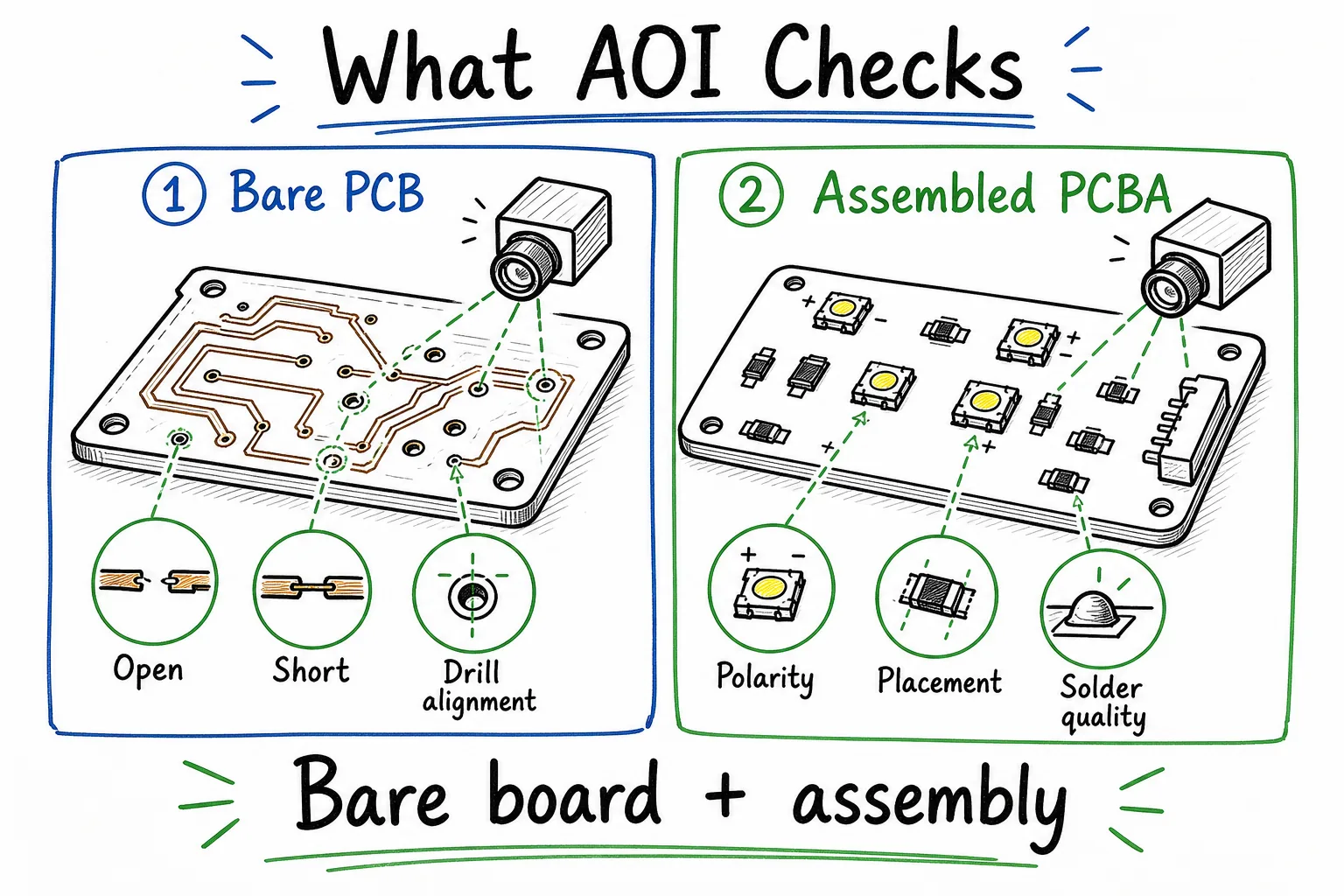 AOI is used during both bare-board PCB fabrication and assembled PCBA inspection.
How AOI Works in Production
At its core, AOI is an automated visual inspection. It does not perform electrical testing; instead, it captures high-definition images of the board surface and compares them to a reference template.
Modern software workflows, such as PCB-Investigator's AOI analysis manual, construct this comparison using a CAD design file, a "golden" (perfect) reference board, or programmed rules. If a board doesn't match the reference criteria, the system flags the area for human review.
The typical AOI workflow follows four phases:
- Image Capture: High-resolution cameras capture the board surface under controlled, multi-angle lighting.
- Comparison: Software compares the captured image against the design template.
- Flagging: Anomalies (like component shift, missing pads, or bridging) are logged.
- Resolution: An operator reviews the flags to confirm whether the board needs repair, must be scrapped, or is a false alarm.
Because AOI relies on visual comparison, its effectiveness depends heavily on lighting, camera angles, and programming rules. It is a highly repeatable tool for catching superficial defects, but it requires proper calibration to avoid missing issues or generating false rejects.
Bare-Board vs. Assembly AOI
AOI is used at two completely different stages in the manufacturing cycle: bare-board fabrication and SMT assembly.
1. Bare-Board Fabrication
During PCB fabrication, we run AOI right after etching and drilling the copper circuit layer. This bare-board inspection is crucial for verifying the physical integrity of the circuit pattern before applying the solder mask or silkscreen. (If you want to learn more about silkscreen guidelines, see our guide on silkscreen design rules).
Catching a copper short or cut at this stage prevents fabricating a defective batch. For fabrication-only orders, bare-board AOI combined with electrical testing forms your primary quality gate.
- Fabrication details: Aluminum PCB fabrication for LED lighting.
2. SMT Assembly
For turnkey orders that include assembly, a second round of AOI is performed after components are placed and soldered. This checks component alignment, solder joint quality, and part presence.
- Assembly details: SMT assembly for LED aluminum PCBs.
- Turnkey services: Turnkey PCB assembly options.
What AOI Can (and Cannot) Detect
AOI is highly effective at catching visible discrepancies, but it cannot verify electrical properties or internal structural issues. Below is a breakdown of what AOI covers across both manufacturing stages.
In Bare-Board Fabrication
During board fabrication, AOI is used to check the etched copper layout against your Gerber design.
- Traces and Spacing: Scans for shorts, opens (cuts in traces), and areas where traces are too narrow or clearances are too small.
- Drilled Holes: Identifies drill breakout where a hole fails to align with its annular ring.
- Missing Features: Flags missing pads or incomplete copper shapes.
[!IMPORTANT] AOI only checks physical appearance. To confirm that the board is electrically functional, manufacturers must perform electrical testing. Standards like IPC-9252B specify electrical testing requirements to verify that unpopulated conductive networks are complete and isolated, regardless of how they look.
In PCB Assembly (PCBA)
During assembly, AOI checks component placement and solder joints against assembly drawings and IPC standards, such as IPC-A-610J.
- Component Placement: Flags missing parts, wrong parts, component skew (shift), or inverted components (tombstoning).
- Soldering Workmanship: Finds visible solder bridges, insufficient solder fillets, or lifted component leads.
- LED Polarity: Checks orientation markings on LEDs. Note that AOI can only verify polarity if the physical LED package has a visible, clear marking that matches the program's template.
Defect Coverage Comparison
| Stage | AOI Focus | Detected Defects | Hidden Limits (Needs Other Testing) |
|---|---|---|---|
| Fabrication | Copper geometry & layout | Traces opens/shorts, clearance violations, breakout | Internal laminate voids, dielectric strength, electrical continuity |
| Assembly | Component placement & solder joints | Missing parts, incorrect polarity, skew, bridges | Hidden joints (e.g., under BGA/QFN), component value, electrical function |
AOI Checkpoints in SMT Lines
AOI can run at multiple points along an SMT assembly line. The most common locations are:
- Post-Solder Paste Printing (SPI): Inspects the height, area, and volume of the printed paste. Catching paste defects early is highly cost-effective, as printing issues cause a large percentage of SMT defects.
- Pre-Reflow AOI: Scans components after placement but before the board goes into the reflow oven. It is easy to reposition or replace components at this stage since the solder paste is still wet.
- Post-Reflow AOI: Checks the board after the solder has melted and solidified. This is the most critical checkpoint because it evaluates the final solder joint quality and catches issues created during reflow (like tombstoning or bridging).
Visual vs. Functional Testing
AOI answers one question: Does the board look right? It cannot answer: Does the board work correctly?
To guarantee reliability, you must pair visual inspection with electrical and functional testing.
| Inspection Method | Purpose | Best For | Limitations |
|---|---|---|---|
| AOI | Automated visual check | Misaligned parts, missing components, visible bridging | Cannot test electrical flow or internal voids |
| Electrical Test (E-Test) | Net connectivity check | Finding hidden opens and shorts | Does not verify component presence or values |
| In-Circuit Test (ICT) | Component-level check | Identifying passive component values and polarities | Requires test points and custom fixtures |
| X-Ray (AXI) | Sub-surface inspection | Inspecting solder joints under QFNs, BGAs, or LED heat pads | Expensive; slower throughput |
| Functional Test (FCT) | Live power simulation | Verifying final board operation (e.g., powering up LEDs) | Doesn't pinpoint exact fabrication errors |
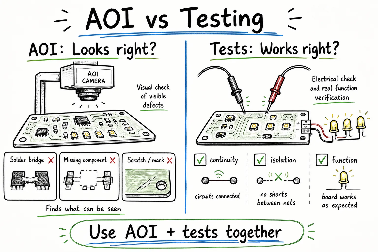 AOI inspects visible features, while electrical and functional tests verify circuit operation.
2D vs. 3D AOI
When reviewing supplier capabilities, you will often see references to 2D and 3D AOI.
- 2D AOI: Captures flat images. It is excellent for checking component presence, text markings, polarity symbols, and locating obvious solder bridging.
- 3D AOI: Uses multiple projection angles to measure height and solder volume. Equipment manufacturers like Koh Young utilize 3D inspection to spot lifted component leads, component tilt, and exact solder joint volume.
For standard single-sided LED aluminum PCBs, 2D AOI is typically sufficient. You do not need to pay a premium for 3D AOI unless your design contains high-density, multi-layer routing, or fine-pitch components (like micro-BGAs). Focus on the supplier's overall defect coverage rather than specific equipment models.
For cost considerations on these designs, see our aluminum PCB cost breakdown.
Supplier AOI Checklist
Do not just ask: "Do you have AOI?" Ask how the inspection is integrated into their quality system. Use these questions to screen potential suppliers:
- Where is AOI applied? Verify if they run AOI on bare boards (post-etching), assembled boards (post-reflow), or both.
- What happens to flagged boards? Confirm they have a closed-loop repair and reinspection process so repaired boards are run back through the scanner.
- What electrical tests follow AOI? A board can look perfect visually but have a hidden short or component failure. Ensure they follow AOI with an electrical test (for bare boards) or a functional lighting test (for LED assemblies).
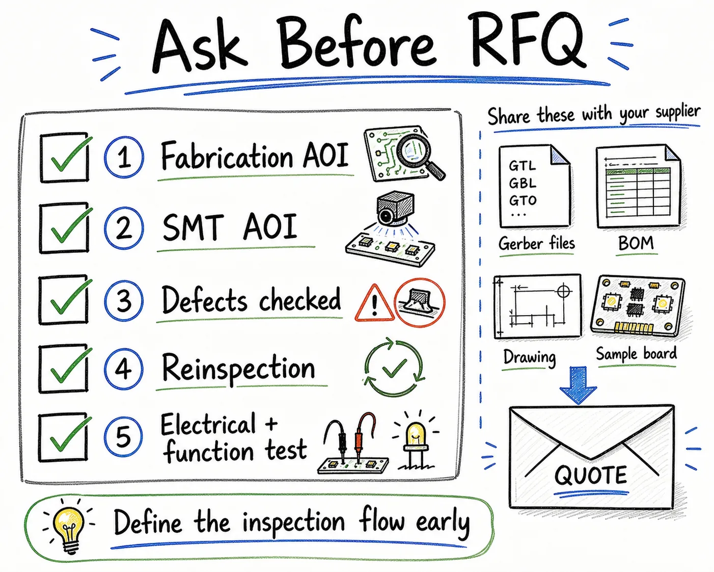 Ask where AOI is used, what it checks, and which tests follow it before quotation.
The Bottom Line
AOI is an invaluable tool for catching visible faults rapidly and consistently, but it is not a standalone quality guarantee. For reliable production, always ensure your supplier combines bare-board and SMT AOI with electrical testing (E-Test) and functional testing.
If you are preparing an LED aluminum PCB design for production, contact us. Send over your Gerber files and BOM, and our engineering team will help you establish a robust testing and inspection plan tailored to your project.
Source Notes
- IPC-A-610J Table of Contents — Acceptability of Electronic Assemblies.
- IPC-9252B Table of Contents — Requirements for Electrical Testing of Unpopulated Printed Boards.
- PCB-Investigator AOI Analysis Manual — 2D/3D optical analysis workflows.
- Koh Young AOI Technology — 3D profilometric measurement.
- Nordson AOI Systems — SMT and PCBA optical inspection.
Join Our Industrial Community
Get exclusive technical whitepapers and industry news delivered to your inbox every month. No spam, only professional insights.