Aluminum PCB Manufacturing Process: 7 Steps You Need to Know

On This Page (Table of Contents)
Ever wonder why two aluminum PCB quotes for the exact same board outline can look completely different?
The difference is hidden in the manufacturing process.
If you are buying LED aluminum PCBs, you don't just need to know how they are made. You need to understand how the process affects your final product's performance and cost.
Specifically, you need answers to these questions:
- Which step determines heat dissipation?
- Which step drives up your costs?
- Which step affects soldering stability?
- Which specifications must you lock down before ordering samples?
When it comes to LED aluminum PCBs, three choices make or break your board:
The dielectric layer, the copper weight, and the surface finish.
These choices determine thermal performance, production yield, lead time, and quotation accuracy.
Let's look at how the 7 manufacturing steps work—and what you need to check at each step to get the best results.
The 7 Steps of the Aluminum PCB Manufacturing Process
Aluminum PCB manufacturing is not just bonding copper onto an aluminum sheet.
It is a full process that starts with material preparation and ends with testing and shipment.
The general structure also matches common IMS and MCPCB manufacturing logic. NCAB's IMS PCB guide and Wurth Elektronik's IMS design rules both treat the metal base, thermal dielectric, and copper circuit as the core stack.
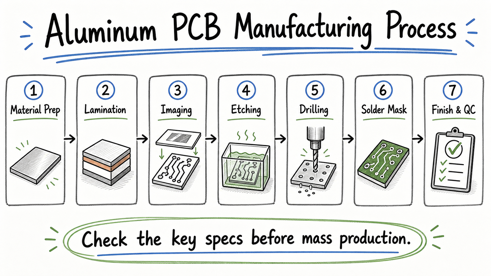 A simple 7-step view of the aluminum PCB manufacturing process, from material preparation to final QC.
For a common single-sided LED aluminum PCB, the process works like this:
| Step | Process | Main Purpose | What You Should Check |
|---|---|---|---|
| 1 | Material preparation | Cut, clean, and prepare the aluminum base | Thickness, flatness, material stability |
| 2 | Dielectric lamination | Bond the thermal insulating layer between copper and aluminum | Thermal conductivity, insulation, cost |
| 3 | Imaging and etching | Create copper traces and pads | Copper weight, trace/space, yield |
| 4 | Drilling and profiling | Make mounting holes, slots, and outlines | Hole accuracy, burrs, assembly fit |
| 5 | Solder mask and silkscreen | Protect copper and mark the board | White solder mask, pad opening, markings |
| 6 | Surface finish | Protect exposed pads for soldering | OSP, HASL, ENIG, storage needs |
| 7 | Testing and QC | Check electrical, visual, dimensional, and reliability items | Stable quality for repeat orders |
Most articles stop after listing these steps.
But if you want to optimize your design and budget, you need to go deeper. You need to know how each step affects your sample, price, and mass production result.
Step 1: Aluminum Substrate Preparation
Aluminum substrate preparation builds the foundation of your board.
The aluminum base supports the circuit mechanically and spreads heat away from your LED components.
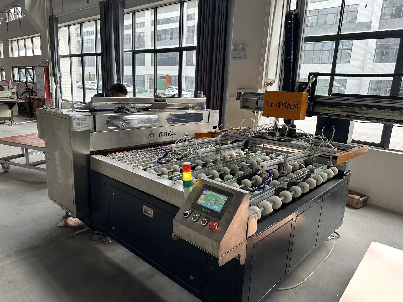 Substrate cutting prepares the aluminum base before later bonding and circuit processing.
Common aluminum materials for LED boards include 5052 and 6061.
5052 is the standard choice for general processing. 6061 has higher tensile strength and is better when your design needs strong mechanical support.
Most LED aluminum PCBs use thicknesses around 1.0 mm to 1.6 mm. Other options like 0.8 mm or 2.0 mm are also common depending on the fixture structure.
But do not judge the board by thickness alone.
Thickness directly affects:
- Mechanical strength
- Heat spreading
- Material cost
- Processing difficulty
- Lead time stability
Before lamination, the factory cleans and preps the aluminum surface.
The goal is simple: the dielectric layer must bond reliably to the aluminum base.
If any oil, oxide, or dust remains, the bonding becomes unstable. In production, this leads to delamination, blistering, or thermal reliability failures.
So, here is what you need to confirm:
- The finished board thickness and tolerance requirements.
- Whether the board must fit a housing or heat sink tightly (requiring high flatness).
- Don't treat aluminum thickness as just a mechanical number—it determines how easily the board fits your final LED fixture.
Step 2: Dielectric Layer Lamination
Dielectric lamination is one of the most critical steps in the entire manufacturing process.
The dielectric layer sits directly between the copper circuit and the aluminum base.
It must do two things at the same time:
- Transfer heat.
- Provide electrical insulation.
The basic stack works like this:
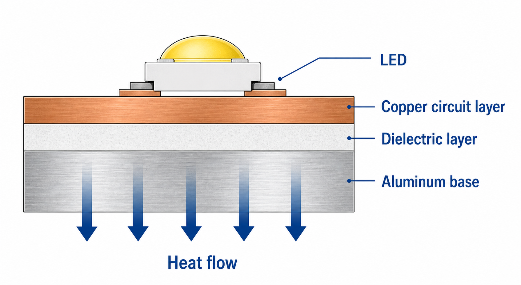 An aluminum MCPCB moves LED heat from the copper circuit layer through the dielectric layer into the aluminum base.
Heat from the LED flows into the copper layer first. Then it passes through the dielectric layer, and finally moves into the aluminum base and your fixture structure.
Here is the problem: the dielectric layer is often your main thermal bottleneck.
If you choose a low-quality dielectric, even a massive aluminum base won't solve your heat problems.
Industry data from Bergquist LED Thermal Solutions, Ventec VT-4B5 SP material data, and Wurth's IMS design rules all point to the same fact: dielectric conductivity, thickness, and breakdown strength are the key items you must specify.
When choosing a dielectric, compare these four factors:
- Thermal conductivity
- Dielectric thickness
- Breakdown voltage
- Material cost and availability
A common assumption is that higher thermal conductivity is always better.
But here is the deal: it isn't.
For standard indoor LED boards, a standard dielectric is usually more than enough. If you pay for a high-conductivity material without a real thermal need, you are just throwing money away.
Use this framework to compare your options:
| Dielectric Option | Typical Thermal Conductivity | Typical Thickness | Cost Level | Practical LED Fit |
|---|---|---|---|---|
| Standard thermal dielectric | 1.0-2.0 W/mK | 100-200 um | Low | Indoor LED boards and low-to-medium power lighting |
| Enhanced thermal dielectric | 2.0-3.0 W/mK | 75-150 um | Medium | Commercial lighting, street lights, higher-power modules |
| High-performance thermal dielectric | 3.0-4.2+ W/mK | 50-100 um | High | High-power LEDs and compact thermal designs |
Before moving to mass production, make sure you lock in the exact dielectric grade, thickness, and thermal conductivity. If these specs shift after you approve the sample, your thermal resistance, insulation behavior, and costs will shift with them.
For example, a low-power indoor LED board doesn't need an expensive 4.2 W/mK dielectric. But a compact, sealed street light module might need it because the housing leaves very little margin for heat dissipation.
Step 3: Circuit Imaging and Etching
Circuit imaging and etching create your copper traces and pads.
The main driver here is your copper weight.
 Circuit imaging defines the copper pattern before etching removes unwanted copper.
Common copper weights include:
- 1 oz (about 35 um)
- 2 oz (about 70 um)
- 3 oz (about 105 um)
Thicker copper carries more current and helps spread heat across the board surface. But it is also much harder to etch cleanly.
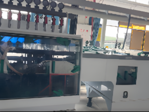 Etching removes unwanted copper and forms the final conductive pattern.
Because etching removes copper chemically, thicker copper means the factory has to dissolve more metal. This requires greater compensation for "undercut" (where the chemical etchant eats away at the sides of the trace).
As a result, heavier copper requires wider trace-and-space design rules, which increases process time and costs.
Here is how copper weight impacts your production:
| Copper Weight | Thickness | Etching Difficulty | Cost Impact vs 1 oz | Practical LED Fit |
|---|---|---|---|---|
| 1 oz | 35 um | Low | Baseline | Low-power LED boards and signal circuits |
| 2 oz | 70 um | Medium | Often about 10-20% higher | Many LED lighting boards |
| 3 oz+ | 105 um+ | High | Can increase clearly due to heavy-copper processing | High-power LED boards and high-current paths |
For most LED lighting boards, 2 oz copper provides a solid balance of performance and price.
But don't default to 2 oz if you don't need it. If your design is low-power and cost-sensitive, 1 oz copper might do the job perfectly.
If your design truly requires 3 oz or heavier copper, confirm it early. Heavy copper directly affects your minimum trace width, etching compensation, solder mask coverage, and final quote.
Step 4: Drilling and Profiling
Drilling aluminum is completely different from drilling standard FR4.
Aluminum is tough on drilling tools, and controlling burrs (rough edges left by the drill bit) is critical.
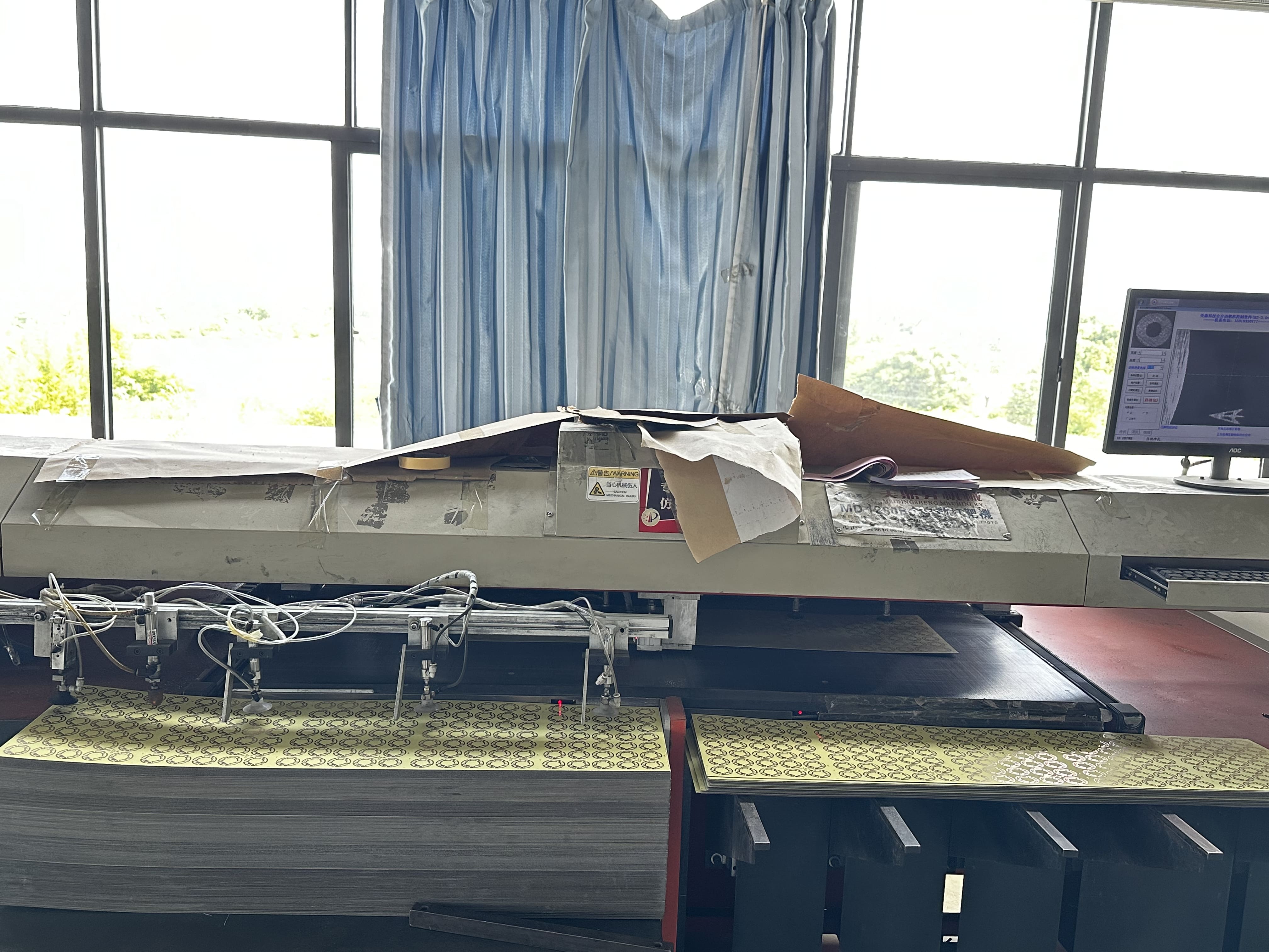 Drilling creates mounting holes, slots, and other mechanical features in the aluminum PCB.
While single-sided LED boards usually have simple hole patterns, tight tolerances or dense slots require extra care.
If tool wear is not monitored, you run the risk of:
- Exit burrs that prevent the board from sitting flat.
- Rough hole edges.
- Hole position shifting.
- Delamination or micro-cracks near the dielectric layer.
These issues might seem minor in a factory photo, but they will cause assembly headaches when you try to screw the board down or slide it into a tight metal housing.
If your board has strict mechanical tolerances, always send a detailed mechanical drawing along with your Gerber files. This allows the factory to verify hole positions, slot tolerances, and outline dimensions before quoting.
Step 5: Solder Mask and Silkscreen
Solder mask protects your copper traces from oxidation and prevents bridging during assembly.
But for LED boards, the solder mask does something else: it acts as an optical reflector.
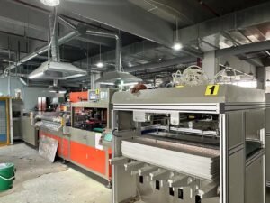 White solder mask is common for LED aluminum PCBs because it supports a clean optical area around LEDs.
This is why most LED boards use a white solder mask. It helps reflect light and keeps the finished luminaire looking clean.
When specifying your solder mask, you should confirm:
- The exact color (glossy white, matte white, or super-white reflective).
- Whether you need a specialized high-reflectivity mask.
- Opening requirements for pads.
- Silkscreen color and character clearance.
- Polarity marks and alignment guides.
Keep in mind that thicker copper makes solder mask coverage harder. High trace edges require precise coating control. If the mask is applied unevenly, you will end up with exposed copper or thin spots that discolor during reflow.
To avoid surprises, approve the white solder mask color and cosmetic standards during the sampling phase. Once you go into mass production, arguing about color shades or coverage is much more difficult.
Step 6: Surface Finish
Your surface finish protects exposed copper pads from oxidation and ensures stable SMT assembly.
For LED aluminum boards, the common choices are OSP, lead-free HASL, ENIG, and Immersion Tin.
Choosing the right finish is a balance between your assembly schedule, pad flatness, storage requirements, and budget. For deeper technical details on finishes and storage behavior, resources like Uyemura's PCB finish FAQ offer practical data, especially regarding ENIG specifications under standards like IPC-4552.
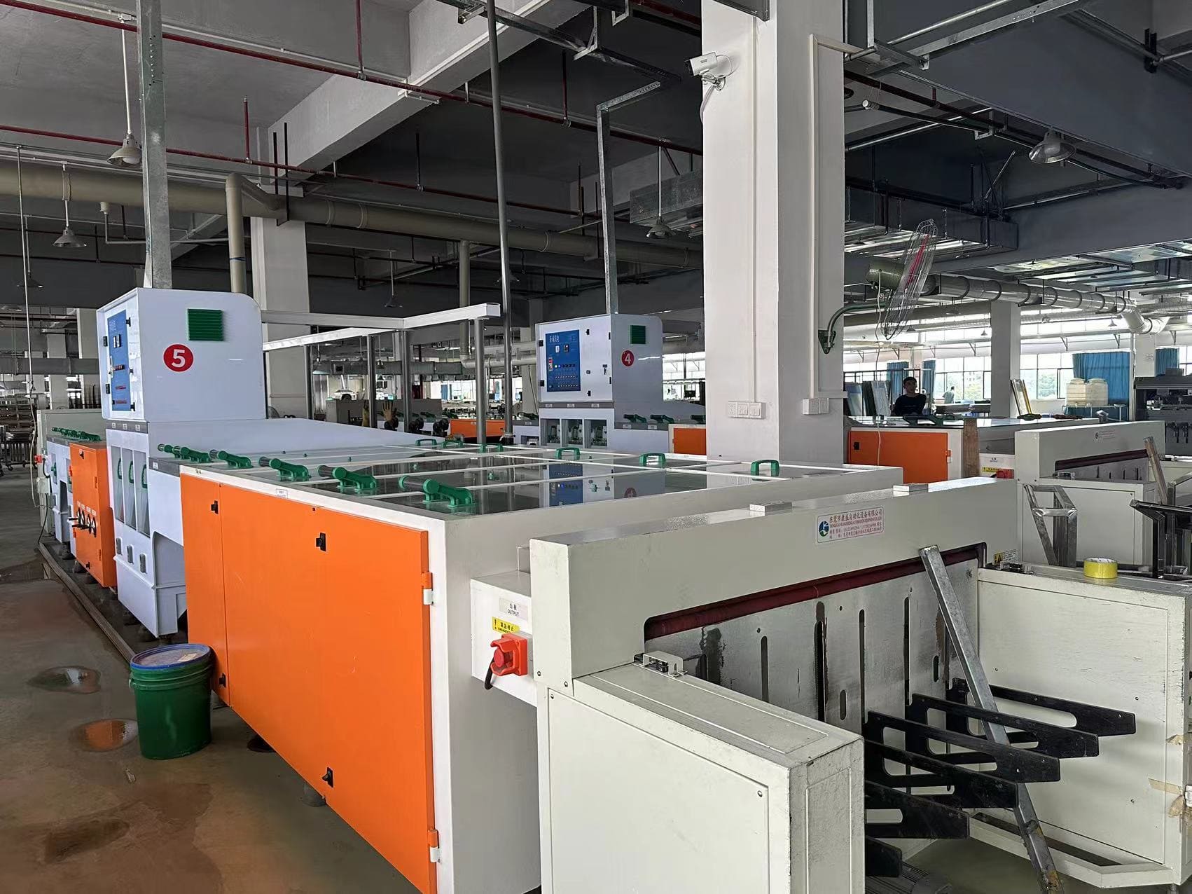 Surface finish protects exposed pads and helps maintain solderability before assembly.
Here is how the finishes compare:
| Finish | Solderability | Flatness | Cost | Storage Behavior | LED Fit |
|---|---|---|---|---|---|
| OSP | Good at first, storage-sensitive | Good | Low | Shorter shelf life, best for fast assembly | Cost-sensitive SMT builds |
| Lead-free HASL | Forgiving in soldering | Less flat | Low to medium | More stable than OSP | General LED boards |
| ENIG | Stable | Good | High | Better storage stability | Fine-pitch LEDs, longer storage, higher reliability |
| Immersion tin | Good | Good | Medium | Medium storage cycle | Short-to-medium cycle builds |
If you want the safest, most reliable option, ENIG is the way to go. It offers excellent flatness and shelf life, though it comes at a premium.
If you are on a tight budget and will assemble the boards immediately, OSP is a solid choice. Just keep in mind that OSP has a short shelf life and is highly sensitive to humidity.
HASL is cost-effective and very easy to solder, but it leaves an uneven surface. If you are using very small LED packages (like 3535 or smaller), HASL's uneven pads can lead to components tilting during reflow.
Align your surface finish with your assembly schedule:
- For fast assembly at lowest cost: Consider OSP.
- For general LED boards with wide soldering tolerance: Consider HASL.
- For fine-pitch LEDs, long storage, and high reliability: Choose ENIG.
Step 7: Testing and QC
Quality control for aluminum PCBs goes far beyond checking for opens and shorts.
Because these boards deal with high temperatures and voltages, you must verify the thermal path and dielectric insulation.
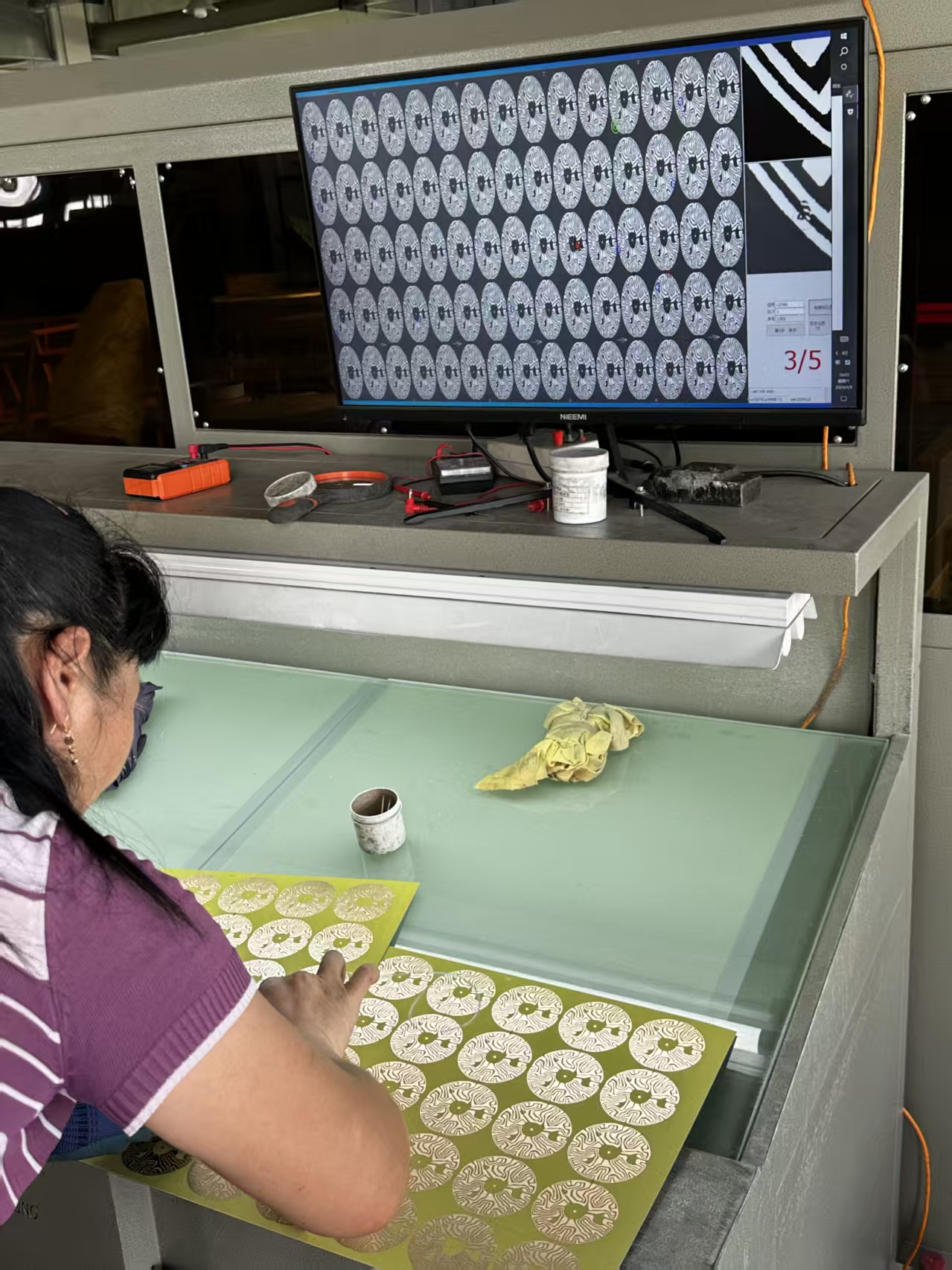 AOI inspection and other inspection steps help catch pattern, solder mask, and workmanship issues before shipment.
While standard production rules usually refer to rigid board specs like IPC-6012, your testing plan should target the specific stresses of your application.
Here is a breakdown of the standard test suite:
| Test | What It Checks | Why It Matters for LED Boards |
|---|---|---|
| AOI | Pattern, spacing, solder mask alignment | Reduces assembly defects |
| Electrical test | Opens, shorts, isolation | Finds electrical issues before shipment |
| High-pot test | Dielectric insulation | Important for safety under driver voltage |
| Microsection | Copper thickness, bonding, hole quality | Checks process interfaces |
| Thermal resistance check | Heat transfer through the dielectric | Helps verify thermal path |
| Thermal cycling | Reliability under temperature stress | Helps reveal delamination or cracking risk |
You don't need to run every advanced reliability test for every simple order. But you must match your testing plan to your operating voltage and environment.
More importantly, remember this: a successful sample batch does not guarantee mass production consistency.
Mass production is a test of repeatability. The factory must deliver the exact same stackup, copper weight, and thermal performance from batch to batch. Make sure you lock in the test requirements during the sample approval stage so there is no deviation during bulk runs.
Sample vs. Mass Production: What Changes?
While the fabrication steps are identical, the factory's internal focus shifts dramatically when transitioning from prototype to bulk production.
The difference is practical. During sampling, the focus is validating that the design works — unit price is higher, lead time is more flexible, and specs may still evolve. Mass production is the opposite: the goal is consistent, repeatable delivery. Price drops as quantity grows, schedules tighten, and every specification should be locked before the run starts. Panel utilization gets optimized, and QC shifts its focus from function and basic dimensions to batch consistency and yield.
Most production delays or failures occur because specifications were not locked down. If you change your copper weight, surface finish, or dielectric material late in the game, you introduce massive yield risks.
Run sample tests first, especially if you are working with high-power LEDs, irregular outlines, or heavy copper boards.
After Manufacturing Comes LED Assembly
Once your bare board is fabricated, it goes to SMT assembly.
This step is just as critical for thermal stability. The solder joints under your LEDs do not just conduct electricity—they are the thermal bridges that carry heat to the aluminum core.
A standard SMT assembly workflow involves:
- Solder paste printing
- Pick and place
- Reflow soldering
- AOI inspection
- Functional testing
If you use separate suppliers for fabrication and assembly, make sure they align on pad design, stencil thickness, reflow profiles, and inspection standards before production begins. Any mismatch here can lead to poor thermal transfer or component misalignment.
What to Prepare Before Requesting a Quote
If you want a fast, accurate quote, sending just the board size and quantity isn't enough. The factory needs your exact specifications to estimate tooling and material costs.
At a minimum, prepare these five items:
- Board thickness and tolerance requirements.
- Copper weight (e.g., 1 oz, 2 oz).
- Dielectric requirements (thermal conductivity, thickness, and voltage breakdown).
- Surface finish (OSP, HASL, or ENIG).
- Order quantity (specifying if it is for samples or mass production).
To get the most accurate quotation, you should also provide:
- Gerber files and NC drill files.
- Mechanical drawings (showing slots, outlines, and tolerances).
- Stack-up notes.
- White solder mask reflectivity requirements.
- Bill of Materials (BOM) and pick-and-place files (if you require SMT assembly).
The more complete your package, the fewer assumptions the factory has to make. This means your quote is faster, more accurate, and has no surprise fees down the road.
If you are evaluating your specifications or ready for a quote, send us your Gerber files and stackup requirements. We will review your board and suggest a practical, cost-effective LED aluminum PCB manufacturing option.
Need a quotation?
Send Gerber files and basic specifications. We reply within 1 business day.
Ask for Quote