PCB Silkscreen Markings & Design Rules: LED Polarity, Clearances & Solder Mask

On This Page (Table of Contents)
Silkscreen carries no voltage and no current. If you scrape it off, copper traces still work.
Still, bad silkscreen causes our most expensive line shutdowns.
One reversed diode string leaves the entire board dark. One drop of ink on a solder pad stops paste from wetting copper. Parts stand up on end, or joints snap during heat cycles.
On aluminum LED boards, silkscreen is not decoration. It is a functional roadmap. Placement cameras, AOI optical scanners, and assembly operators all rely on it to build boards fast.
What Belongs on Your Silkscreen (And What to Drop First)
Every printed letter takes up board space. On narrow linear strips and compact downlights, surface area runs out fast.
Keep five core markings on your board:
- Reference designators (
LED1,R1,C3) match parts to your BOM. - Polarity indicators show diode direction before and after reflow.
- Pin-1 markers orient ICs and multi-pin wire connectors.
- Terminal pinouts label DC power connections (
+24V,GND,PWM). - Board revision codes (
Rev B2) keep outdated boards off the line.
Shop floor rule for tight layouts. When space is tight, drop logos and decorative frames first. Never drop a reference designator or a polarity mark to fit a logo.
SMD LED Polarity Silkscreen and Why One Tiny Dot Fails
LED orientation errors cause frequent rework on SMT lines.
The root cause is simple. LED makers do not follow one polarity standard.
On common 2835 and 3030 packages, one vendor notches the cathode lead frame while another notches the anode. EDA libraries in Altium, KiCad, and Eagle disagree just as often. They frequently swap Pin 1 between anode and cathode.
If your Gerber drawing shows only a single dot, the programmer must guess. A wrong guess leaves an entire production batch unlit.
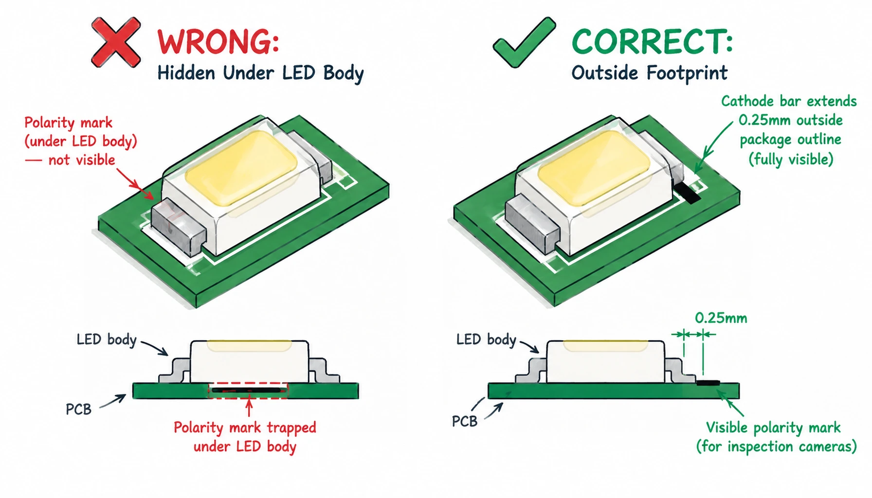 SMD LED polarity markings must sit outside the package footprint so operators and AOI cameras can verify orientation after reflow.
Four Clear Ways to Mark LED Polarity
Stick to these verified silkscreen styles on the production line.
| Marking Style | Visual Description | Layout Placement | Recommended Use |
|---|---|---|---|
| Cathode Bar | Solid silkscreen line parallel to the terminal | 0.25 mm outside the cathode pad | 0603, 0805, 1206 chip LEDs & indicator arrays |
| Footprint Chamfer | Silkscreen outline matches the package notch | Matches physical LED package corner | 2835, 3030, 5050 mid-power LED packages |
| Diode Schematic Symbol | Standard triangle pointing to a vertical bar | Triangle points in forward current direction | Discrete diodes, driver boards, dense layouts |
Polarity Text (+ / -) | Bold plus and minus characters | 0.50 mm beside solder lands or terminals | Long linear boards, COB arrays, and DC lines |
Keep Polarity Marks Outside Component Outlines
The most common silkscreen error is placing a polarity dot under the LED body.
In CAD at 800% zoom, the dot looks clear. Once the board clears the reflow oven, the LED package covers it completely.
That hidden mark blocks inspection.
- AOI cameras cannot verify diode orientation.
- Technicians cannot spot reversed LEDs during first-article inspection.
- When a string fails, workers must probe every diode with a multimeter.
Aluminum boards pull heat away fast. Desoldering requires high heat that scorches white solder mask. Always place polarity marks at least 0.25 mm outside the LED package outline.
DFM Clearances for Pad and Line Spacing
Board shops enforce clearance limits for practical physical reasons.
During production, liquid inks spread, and printing screens stretch under mechanical squeegees.
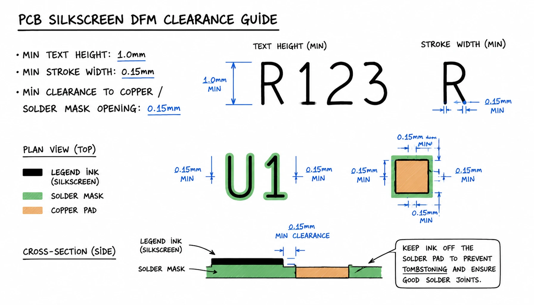 Silkscreen DFM rules maintain safe clearance from solder mask openings, preserving minimum stroke widths to prevent broken letters and pad contamination.
Why Pad Contamination Causes Tombstoning
The most expensive silkscreen defect is ink overlapping an exposed copper pad.
Silkscreen ink is an organic polymer. Molten solder will not wet it.
When ink bleeds onto a pad, solder paste cannot bond to copper. Uneven surface tension pulls small two-pin parts upright into tombstones. On center LED thermal pads, trapped ink boils off and creates large solder voids.
Shop Floor Clearances You Must Keep
Keep your layout within these boundaries.
| Dimension / Clearance | Recommended Target | Absolute Minimum | Shop Floor Failure Risk |
|---|---|---|---|
| Text Height | 1.20 mm – 1.50 mm | 1.00 mm (39 mil) | Letters close up and blur into illegible dots |
| Stroke Width | 0.18 mm – 0.20 mm | 0.15 mm (6 mil) | Lines break and flake off during chemical washing |
| Pad Clearance (To Mask Opening) | 0.20 mm (8 mil) | 0.15 mm (6 mil) | Ink encroaches onto pads; solder fails to wet |
| Copper Clearance | 0.25 mm (10 mil) | 0.20 mm (8 mil) | Registration drift risks printing onto bare copper |
| Board Edge / V-Cut Margin | 0.80 mm (31 mil) | 0.50 mm (20 mil) | Scoring blades shred text into unreadable pieces |
Watch Out for Gerber Auto-Clipping
Before imaging, factory CAM engineers run automated scripts to trim silkscreen off bare copper.
This clipping protects solder pads, but it can ruin text. A plus sign (+) placed too close to a pad loses its crossbar and becomes a minus sign (-). A label like LED12 gets clipped into ED12 or plain 12.
Set your CAD DRC rules to keep at least 0.15 mm between silkscreen text and solder mask openings.
How Factories Print Silkscreen
PCB shops print markings using three standard methods.
1. Semi-Automatic Screen Printing
This is the standard choice for linear LED boards. A squeegee pushes epoxy ink through a woven mesh stencil. It gives thick, opaque ink at the lowest cost. Mesh stencils stretch over long panels, which creates registration drift and limits lines to 0.18 mm.
2. Liquid Photo Imaging (LPI)
Photo-imageable ink covers the panel, dries, and develops through film tools. It produces sharp edges down to 0.12 mm stroke widths. The extra chemical steps add setup cost, so shops rarely run LPI on standard lighting boards.
3. Direct Legend Printing (DLP / Inkjet)
Printheads spray UV-curable ink directly from CAD data, and UV lamps cure droplets instantly. DLP avoids stencils and mesh stretch, reaching accuracy and 0.10 mm fine lines. It is ideal for serialized QR codes, barcodes, and dense boards.
PCB Silkscreen vs. Solder Mask
Buyers sometimes mix up silkscreen and solder mask. Both are liquid coatings, but they perform opposite jobs.
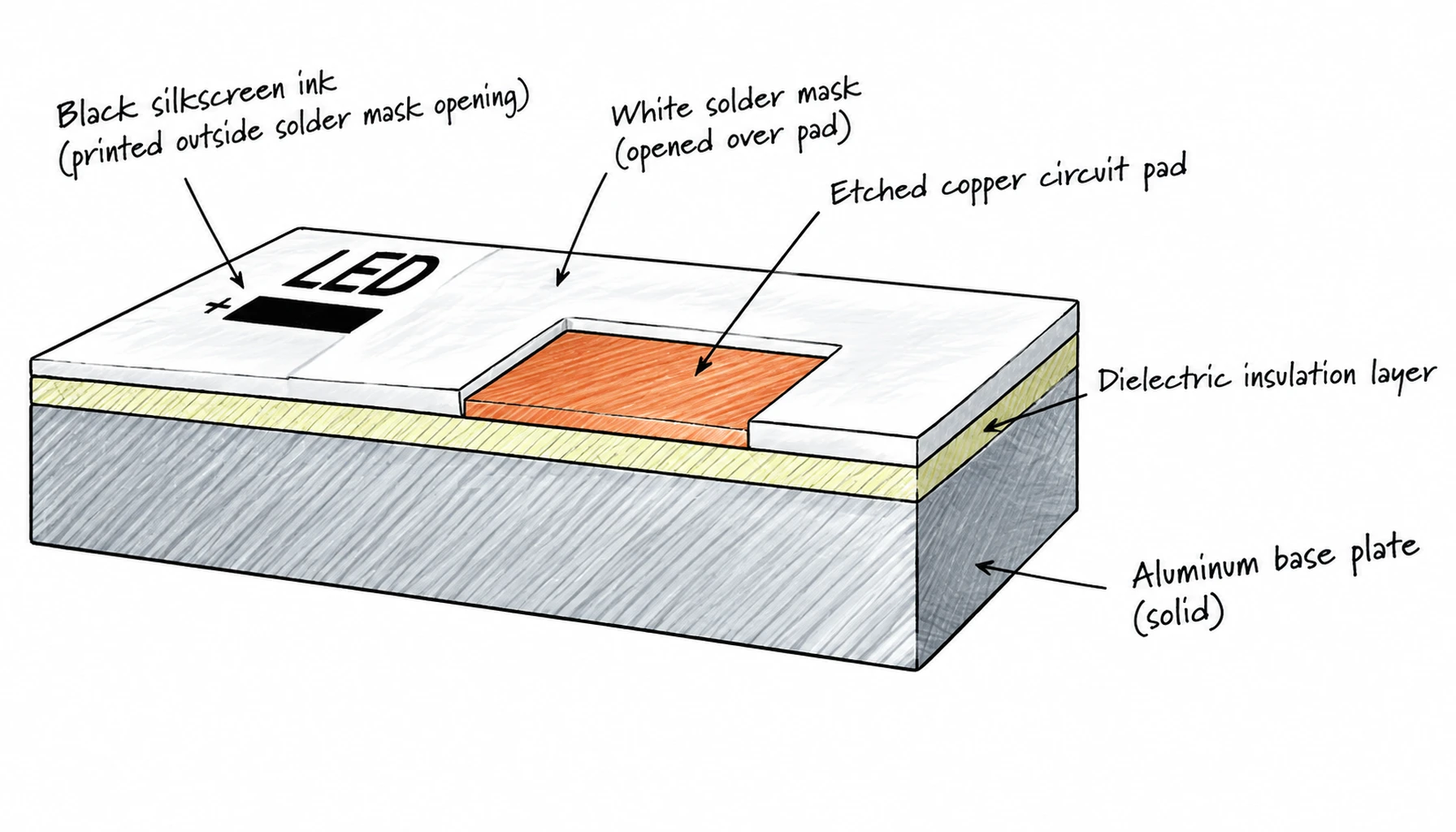 Solder mask forms a protective insulation barrier across copper traces, while silkscreen is printed on top to provide human and machine identification.
Solder mask is an electrical insulation barrier. Factories apply it directly over bare copper, opening windows only over solder pads. It prevents solder bridging between traces and protects copper from oxidation.
Silkscreen is purely an informational layer. Shops print it directly over the cured solder mask. Silkscreen ink has zero rated dielectric strength. Never rely on silkscreen to insulate electrical tracks.
| Characteristic | Solder Mask Layer | Silkscreen (Legend) Layer |
|---|---|---|
| Primary Function | Electrical insulation, solder bridging prevention, moisture shield | Visual component identification, polarity, tracing, pinouts |
| Material Base | Liquid Photo-Imageable (LPI) epoxy resin | Thermally cured epoxy or UV-cured acrylic ink |
| Application Order | Applied before surface finishes (HASL, ENIG, OSP) | Applied after solder mask cure; before or after finish |
| Typical Thickness | over copper traces | raised ink profile |
| Electrical Insulation | High dielectric strength () | None specified; purely non-conductive visual layer |
| Standard Colors | High-reflectivity White (LED), Green, Matte Black | Black (on white mask), White (on green/black mask), Yellow |
Three Silkscreen Hazards on Aluminum LED Boards
Metal-core PCBs (MCPCB) present three assembly risks you rarely see on standard FR4 boards.
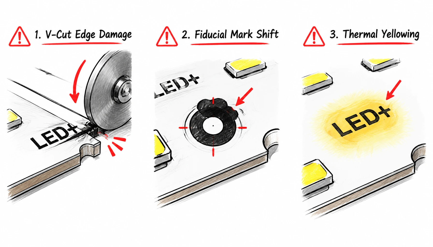 MCPCB silkscreen hazards include V-cut blades clipping edge text, ink encroaching on fiducial marks, and low-grade ink yellowing.
1. High-Reflectivity White Mask and Ink Yellowing
LED fixtures rely on white solder mask with 88% to 92% optical reflectance. White mask requires high-contrast black text.
Lead-free reflow reaches peak temperatures of . Low-grade black inks release solvents into the hot white mask, creating yellow halos around text. That yellowing drops reflectance by 5% to 8%, shifting luminaire lumen output and color temperature (CCT). Always specify non-yellowing legend ink tested for lead-free reflow.
2. The 0.5 mm V-Cut Scoring Shredder
Linear lighting strips often measure 0.6 m to 1.2 m in length. Factories separate finished panels with rotating steel blades that cut V-grooves from both sides.
Blades shred any text printed within 0.50 mm of the cut line. If a cut destroys a + or - label, assembly workers must guess wire polarity. Reverse wiring instantly blows driver circuits. Keep all legend text and test points at least 0.80 mm away from scorelines.
3. SMT Optical Fiducial Contamination
Pick-and-place machines align aluminum boards using optical fiducials. These are small copper pads surrounded by a clear solder mask ring.
Vision cameras find board edges by checking contrast between copper and white mask. If silkscreen sits within 1.0 mm of the fiducial ring, cameras lock onto the ink edge by mistake. That false lock shifts the whole panel offset, moving LED leads off their solder pads. Keep a clean 1.0 mm radius around every fiducial target.
What to Check Before Sending Gerbers
A clean silkscreen layout costs nothing extra. Still, it prevents line shutdowns, protects optical output, and eliminates manual multimeter probing.
Before releasing Gerber files (.GTO for top legend) for metal-core PCB fabrication or turnkey LED assembly, check these six points:
- Polarity marks outside packages. Keep marks visible after reflow.
- Text sizes meet minimums. Keep height and stroke .
- Pad clearance is safe. Maintain spacing from solder mask openings.
- V-score edges are clear. Keep text away from panel scorelines.
- Fiducials are isolated. Maintain a 1.0 mm clear radius around optical targets.
- High-contrast ink chosen. Use black ink on white mask and white ink on dark boards.
Need a quotation?
Send Gerber files and basic specifications. We reply within 1 business day.
Ask for Quote