Single Layer Aluminum PCB Stackup: The Standard Layer Breakdown & LED Design Rules

On This Page (Table of Contents)
Let’s cut straight to the point.
A single-layer aluminum PCB isn't complicated. It’s essentially a three-layer sandwich:
Circuit copper on top. A paper-thin dielectric in the middle. A solid aluminum slab on the bottom.
Cover the top with reflective white solder mask, slap a peelable blue plastic film on the back to stop scratches, and you’re done.
Over 95% of volume LED boards use this exact build.
Why?
Because heat takes the shortest possible path: straight down from your LED thermal pad into the fixture housing. No plated through-holes. No internal layer delamination. Low manufacturing cost.
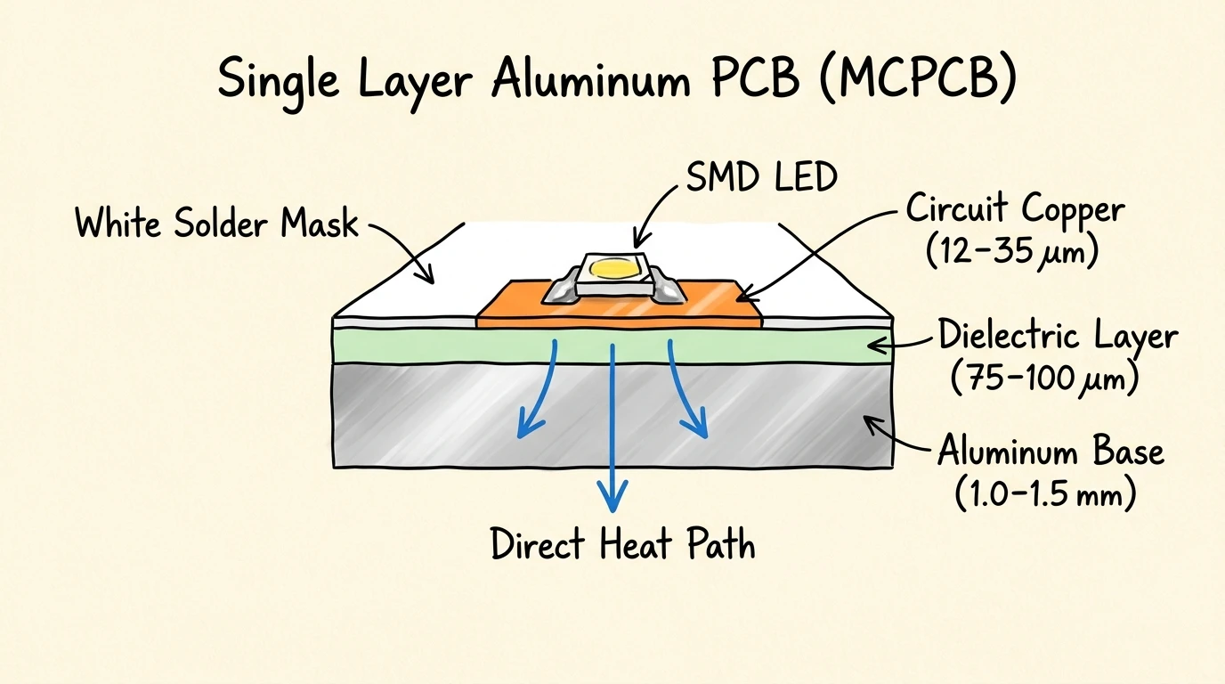 A standard single-layer aluminum PCB stackup. Heat travels straight down through circuit copper and the thin dielectric into the aluminum base plate.
The Layers Inside the Board
Don't picture a bare sheet of aluminum with traces printed on metal.
It’s an asymmetric laminate. The board shop takes copper foil, a thin prepreg film, and an aluminum plate, then bakes them together under high pressure.
| Layer | Common range | Practical role |
|---|---|---|
| White solder mask | 15–25 µm | Reflects fixture light (85–90%), prevents oxidation |
| Circuit copper | 12–70 µm | Carries drive current and LED footprints |
| Dielectric layer | 50–100 µm | Blocks electrical voltage while transferring heat |
| Aluminum base plate | 1.0–1.5 mm | Structural support, spreads heat into luminaire |
| Backside film | ~75 µm PET | Removable foil; stops handling scratches |
Watch out for copper thickness in volume lighting
Your quotation might say "0.5 oz copper" (~18 µm).
In reality? High-volume commercial lighting boards often run on raw laminate with copper closer to 12 µm (~1/3 oz).
For a 40 W commercial troffer or low-current LED strip, 12 µm is completely fine. Traces are wide, currents are low, and thin copper shaves dollars off every square meter.
The trouble starts when you design high-power arrays that push thermal and DC current limits.
If your UL temperature rise test depends on true 18 µm or 35 µm copper, never rely on a verbal agreement. Put the minimum finished copper thickness right on your fabrication drawing—especially when traces run near standard copper trace width and current limits for high-bay or stadium fixtures.
The Dielectric Bottleneck: Thermal Resistance vs Hi-Pot
The dielectric layer is where your heat gets stuck.
Conduction through this thin layer comes down to basic physics:
Where is layer thickness, is thermal conductivity, and is your LED pad area.
Want lower thermal resistance? You have two choices: buy a higher- dielectric, or make the layer thinner.
High- ceramic resin gets expensive fast. Making the layer thinner is cheap—but it eats away your electrical safety margin.
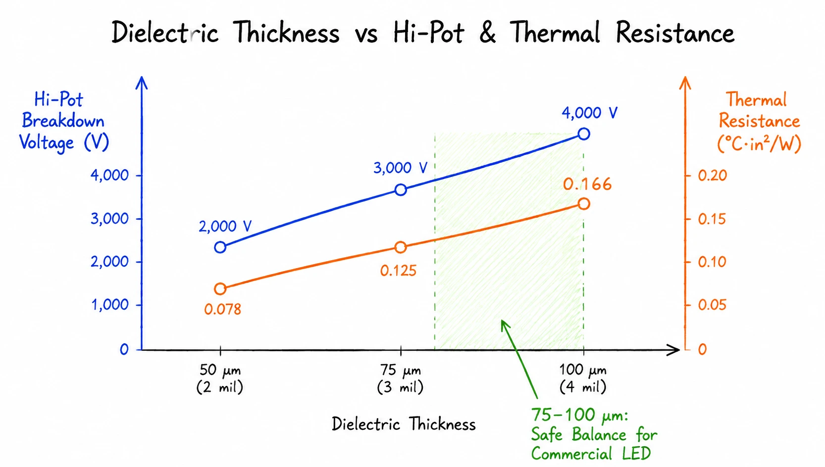 Dielectric thickness trade-off. While thermal resistance rises modestly between 75 and 100 µm, breakdown voltage climbs significantly, giving valuable Hi-Pot safety margin.
Take a look at how this plays out in published laminate data. Ventec’s VT-4B1 datasheet, a benchmark material for LED substrates, maps out this exact balance:
- 50 µm (2 mil): 0.078 °C·in²/W thermal impedance, with 2,000 V DC breakdown.
- 75 µm (3 mil): 0.116 °C·in²/W thermal impedance, with 3,000 V DC breakdown.
- 100 µm (4 mil): 0.166 °C·in²/W thermal impedance, with 4,000 V DC breakdown.
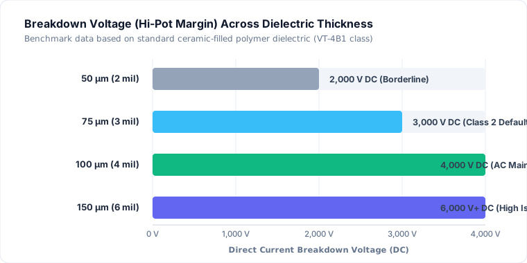 Dielectric breakdown voltage comparison. Stepping from 75 µm to 100 µm increases isolation safety margin by 1,000 V, making boards resilient against micro-cracks during depaneling.
Notice what happens when you step up from 75 µm to 100 µm?
Thermal impedance goes up by roughly 0.05 °C·in²/W. On a typical mid-power LED pad, that shifts your junction temperature by less than 1 °C.
You’ll barely see that on a thermocouple.
What do you gain in return? 1,000 V of extra insulation safety.
Here's why that matters on the production floor.
Super-thin dielectrics (≤50 µm) can’t take mechanical punishment. When your board shop V-scores or punches the panels, micro-cracks form along the edges.
The moment your assembled luminaire hits the factory Hi-Pot test (1,500 V to 3,000 V AC), those cracks arc over. Your finished board is instant scrap.
The practical rule of thumb: 75 µm works for low-voltage Class 2 drivers. If your board connects to direct AC mains, stick with 100 µm as your default baseline so finished fixtures clear production testing without riding borderline dielectric thickness margins. You can model the layer-by-layer temperature rise across your exact stackup with our free LED Junction Temperature Calculator.
5052-H32 vs 1060 Aluminum Base
On paper, pure 1060 aluminum looks like a no-brainer: over 200 W/m·K compared to just 138 W/m·K for 5052-H32.
On an actual production line? Pick 5052-H32 almost every time.
The aluminum base plate only accounts for about 10% of your total junction-to-air thermal resistance. Your solder joints and dielectric layer absorb the rest.
Swapping a 138 W/m·K base for a 200 W/m·K one rarely changes your operating temperature by more than 0.3 °C in bench tests.
Where you will feel the difference is mechanical stability.
- Reflow warpage. Run a 600 mm or 1200 mm strip through a 250 °C lead-free reflow oven. Soft 1060 aluminum sags and bows under heat. 5052-H32 has much higher yield strength—it stays flat through the tunnel.
- Burr formation. 1060 is soft and gummy. When blades cut or V-score it, the metal drags and leaves tall burrs. 5052-H32 shears cleanly.
- Handling stiffness. At 1.0 mm or 1.5 mm, 5052 keeps its shape when workers snap boards into architectural extrusions. Only when you push past extreme heat flux on dense COB clusters does the aluminum base itself become the bottleneck, forcing a switch to copper core MCPCBs.
Why 2-Layer Aluminum Boards Are Rare in LED Lighting
Almost every LED luminaire you see stays on single-layer aluminum.
It comes down to two things: heat stacking and drilling costs.
On a single-layer board, heat takes one clean jump: LED pad copper dielectric aluminum plate.
On a 2-layer aluminum board, that heat has to fight through two separate dielectric barriers:
That second layer of prepreg roughly doubles your thermal resistance.
Then comes the real headache: plated through-holes (PTH).
You can't just drill through aluminum and plate copper down the barrel. That would short every trace straight into the metal core.
To insulate those holes, the board shop has to run a painful four-step process.
- Drill oversized clearance holes through the aluminum plate.
- Fill every hole with insulating epoxy plug resin and bake it solid.
- Re-drill smaller holes dead center through the cured resin plugs.
- Chemically plate copper through the insulated resin sleeves.
All that extra handling sends scrap rates through the roof. A 2-layer aluminum board usually ends up costing three to five times more than a standard single-layer board.
What do lighting designers do when traces have to cross?
They drop in 0-ohm SMD jumpers or zero-ohm bridge resistors. A 0805 zero-ohm jumper costs a fraction of a cent and keeps your board on a cheap single-layer quote.
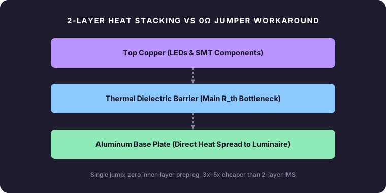 Why single-layer aluminum dominates LED volume: a single thermal jump straight to the base plate avoids the double prepreg thermal trap and multi-step plugged-hole cost.
CAD and DFM Rules for KiCad and Altium
Your EDA software is tuned for multi-layer FR-4 by default.
If you don't adjust your project settings upfront, your DRC will throw endless errors about unrouted bottom nets and missing thermal vias.
Here is how to set up your project cleanly.
- SMD pads only. Turn off electrical vias. A standard single-layer aluminum board cannot take through-hole pins or plated vias. Non-plated mounting holes (NPTH) for screws and alignment pins are fine.
- Edge clearance (≥0.8 mm). Keep all copper traces at least 0.8 mm to 1.0 mm away from outer board edges and V-score cut lines. Scoring blades have a ±0.1 mm tolerance. Route copper too close to that line, and the blade will expose raw copper that arcs over during Hi-Pot testing.
- Clean Gerber package. Export only what’s needed: Top Copper (.GTL), Top Solder Mask (.GTS), Top Silkscreen (.GTO), Board Outline (.GKO/.GM1), and Drill File (.DRL) for NPTH holes only.
- Ditch empty bottom layers. Don't send empty Bottom Copper (.GBL) or Bottom Solder Mask (.GBS) files. CAM engineers see those files and put your order on hold to ask if you forgot your inner layers.
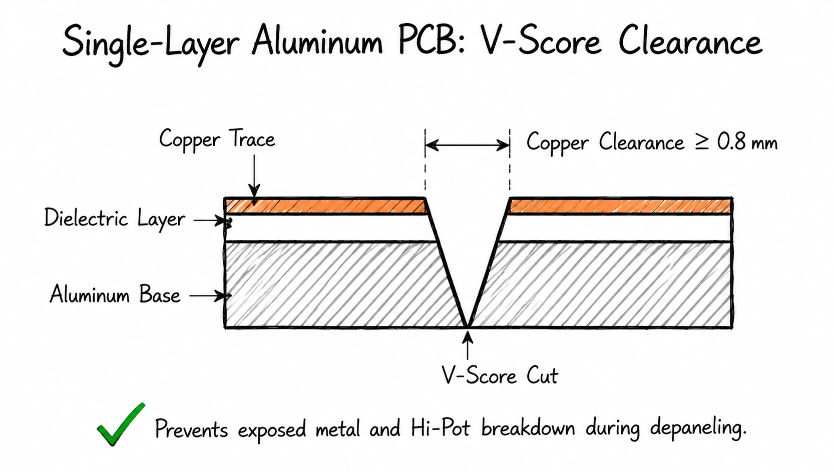 Single-layer aluminum PCB edge clearance. Keeping copper traces at least 0.8 mm away from the V-score cut line prevents exposed metal and Hi-Pot arc-over.
Save yourself an email chain by copying this exact stackup block into your fabrication drawing notes:
1-Layer Aluminum PCB
Total Thickness: 1.5 mm (±0.1 mm)
Base Alloy: 5052-H32
Finished Copper: 1 oz (35 µm)
Dielectric: 100–200 µm (0.6–0.8 W/m·K volume baseline or ≥1.0 W/m·K commercial, breakdown ≥3000 V AC)
Solder Mask: Gloss White
Surface Finish: OSP (or Lead-free HASL)
Three Standard LED Stackup Baselines
Most LED designs fit into one of three standard configurations. Pick the one that matches your drive current and operating voltage.
| Fixture type | Circuit copper | Dielectric layer | Aluminum base | Typical Hi-Pot | Main tradeoff |
|---|---|---|---|---|---|
| Commercial Linear / Troffer | 12 µm (~1/3 oz standard) | 75–200 µm @ 0.6–0.8 W/m·K | 1.0 mm 1060 / 5052 | 1,500–3,000 V AC | Lowest cost per meter (volume baseline) |
| Architectural Downlight / Panel | 35 µm (1 oz) | 100 µm @ 1.5 W/m·K | 1.5 mm 5052-H32 | 3,000 V AC | Balanced stiffness, heat, and Hi-Pot margin |
| High-Power High-Bay / Outdoor | 70 µm (2 oz) | 100 µm @ 2.0 W/m·K | 1.6 or 2.0 mm 5052 | 3,000 V+ AC | High DC current with dense LED clusters |
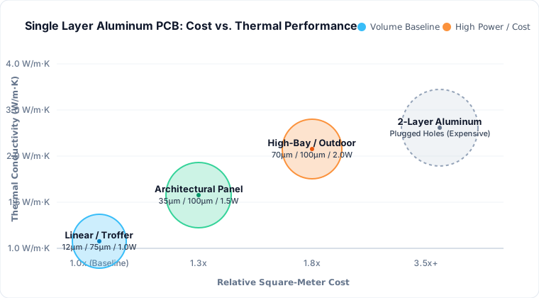 Square-meter cost vs thermal conductivity trade-off. Linear boards prioritize baseline economy, while high-power fixtures invest in thicker copper and higher-k dielectric.
When you specify finished copper, dielectric rating, alloy grade, and total thickness directly on your drawing, your board shop CAM team won't have to pause your job to send clarifying emails. That is how you keep rapid PCB prototyping on schedule without surprise redesign cycles.
Need a quotation?
Send Gerber files and basic specifications. We reply within 1 business day.
Ask for Quote