PCB Prototyping: How to Optimize Tooling Fees When Scaling to Volume Orders

On This Page (Table of Contents)
You want to get your new LED lighting product to market fast.
So you order a cheap prototype run to test your layout.
The sample boards arrive, you solder them in the lab, and they light up fine.
But when you transition to mass production, you face a major obstacle: high tooling setup charges, or boards failing hipot tests.
Why does this happen?
Because prototyping is more than just making a sample work in a lab.
If you ignore the transition to volume production early on, small design errors can turn into expensive mass production costs.
Here is a practical look at how PCB prototyping works, how panel sharing saves you money, and how to avoid tooling and material traps when you scale.
What Is PCB Pooling & How It Lowers Prototyping Costs
To make early-stage R&D affordable, factories use a method called PCB pooling, or panel sharing.
The concept is simple: instead of running a custom production line for your board alone, we combine multiple customer designs on a single standard panel.
By sharing the panel space, you split the upfront setup and film charges.
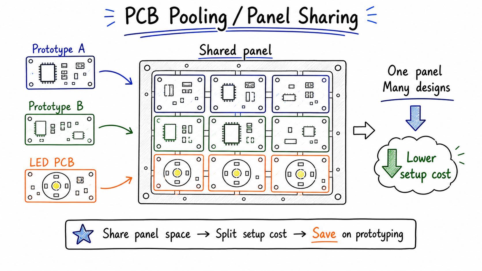 Panel sharing combines multiple prototype designs on one standard panel, helping split setup costs during early PCB prototyping.
But pooling only works if your design fits standard, pre-set parameters.
For single-sided aluminum PCBs, this means matching standard parameters:
- A board thickness of 1.6 mm.
- A copper foil weight of 1 oz (35 um) or 0.5 oz (18 um).
- A thermal conductivity of 1.0 to 1.5 W/mK.
- A standard OSP or HASL surface finish.
If your design requires custom board thicknesses or high-end specs, it cannot be pooled.
But if you design within these standard parameters, pooling is the most cost-effective way to run your first tests.
Why Material Consistency Matters in Aluminum PCB Prototyping
For high-power LEDs, a prototype test is only useful if the volume production boards use the exact same materials.
The dielectric layer is the main factor in heat transfer.
If you test your prototype on a high-conductivity core, but scale production using a cheaper, lower-grade substrate, your thermal tests are no longer valid.
The thermal conductivity could drop from 1.8 W/mK to 0.8 W/mK, causing your LEDs to overheat, lose brightness, or fail early.
Insulation safety is also tied to material thickness.
Under IPC-TM-650 test standards, a 150 um dielectric can support a much higher breakdown voltage than a thinner 75 um layer.
If your prototype passed safety tests on a thicker dielectric, but the mass production run uses a thinner layer to save cost, the board may fail safety certifications.
The assembly process matters too.
Hand-soldering a prototype in a lab is low-stress.
But automated SMT reflow lines apply severe thermal stress.
OSRAM reflow soldering guidelines recommend keeping heating rates below 3 deg C/s to prevent thermal shock to the LED chips and substrate.
If your prototype SMT profile and stencil design are not matched to the volume line, you face solder failures during bulk runs. This is why we align SMT profiling early on for all our SMT assembly for LED aluminum PCB runs.
| What Buyers Should Check | Why It Matters for LED Boards | Factory Practice |
|---|---|---|
| Material Grade | Prevents shifts in thermal conductivity, such as 0.8 vs 1.8 W/mK. | Substrate specifications are kept consistent from prototype to volume runs. |
| Dielectric Thickness | Affects insulation breakdown voltage and safety margin. | Thickness is controlled to match safety and hipot standards. |
| SMT Oven Profiles | Prevents solder voiding and thermal shock to LED chips. | Reflow profiling is aligned between sample testing and volume runs. |
| DFM Alignment | Ensures design parameters translate to mass production. | A free engineering review is performed before prototype fabrication. |
In our experience with aluminum PCB fabrication for LED lighting, using consistent, traceable substrate materials for both prototypes and volume runs is the only way to ensure your testing data remains valid as you scale.
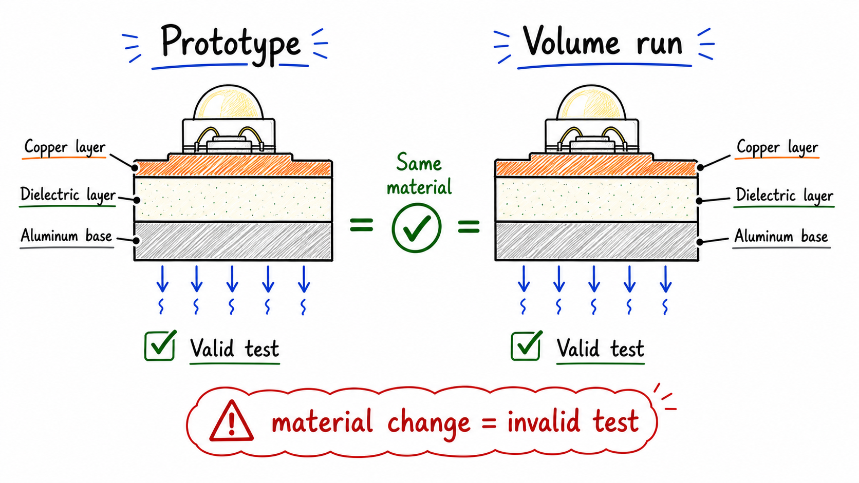 Prototype data stays useful only when the volume run keeps the same copper, dielectric, and aluminum base material stack.
CNC Routing vs. Punching Die: Why Edge Clearing Rules Change for Mass Production
During prototyping, your boards are cut using CNC routing, or milling. While CNC routing is highly precise (tolerances of ±0.1 mm), the mechanical routing bit can sometimes leave tiny copper burrs along the board edge if your copper traces are laid out too close to the perimeter.
But CNC routing is too slow for volume orders.
For mass production, factories switch to V-scoring or punch die stamping. Punch die stamping uses a custom steel tool to shear boards apart instantly, which is highly efficient.
Under safety standards like IEC 60664-1 and IPC-2221B, the board edge acts as an insulation boundary. To prevent exposed copper and maintain high insulation reliability, a standard 0.5 mm copper-to-edge clearance is verified during the design-for-manufacturability (DFM) check stage for most single-sided LED aluminum PCBs.
However, a standard 0.5 mm clearance is not a universal rule. A custom clearance review is required before mass production if your design features:
- Special shaping or routing methods.
- An extremely narrow board width.
- High-voltage areas requiring larger creepage distances.
- Specific reliability requirements from the end-customer.
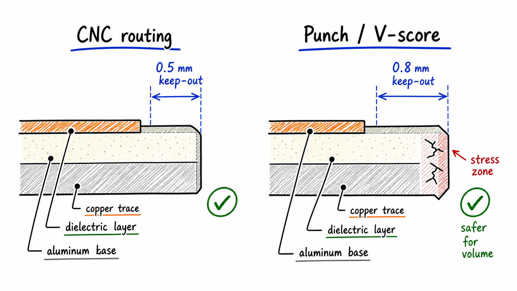 A DFM review verifies a standard 0.5 mm trace-to-edge spacing for most LED boards, adjusting the keep-out distance for special parameters like high voltage or narrow widths.
These spacing rules are detailed in the TI High-Voltage Spacing Guide, which explains why board edges are critical insulation boundaries. Designing with these manufacturing variables in mind ensures a smooth transition from routed prototypes to stamped volume runs without layout revisions right before production.
Commercial Tooling Cost Models: How to Offset Setup Fees When Scaling
Transitioning a hardware project from prototype to volume production requires physical tooling, often called non-recurring engineering, or NRE, fees.
These cover photo-plotter films, solder stencils, and custom steel punch die molds.
Many buyers focus solely on unit price and get blindsided by these upfront setup charges.
A cheap unit price offset by a massive tooling fee can increase your total cost of ownership, or TCO, if your volume is lower than expected.
Furthermore, changing suppliers between prototyping and volume runs is a common B2B mistake.
A new factory must recreate the tooling, run first-article checks, and recalibrate SMT reflow profiles. Any slight variance in their material dielectric can invalidate your previous thermal tests.
To help manage your development budget, direct factories often offer commercial credits.
For example, the prototype setup fees can be credited back against the invoice of the subsequent mass production order.
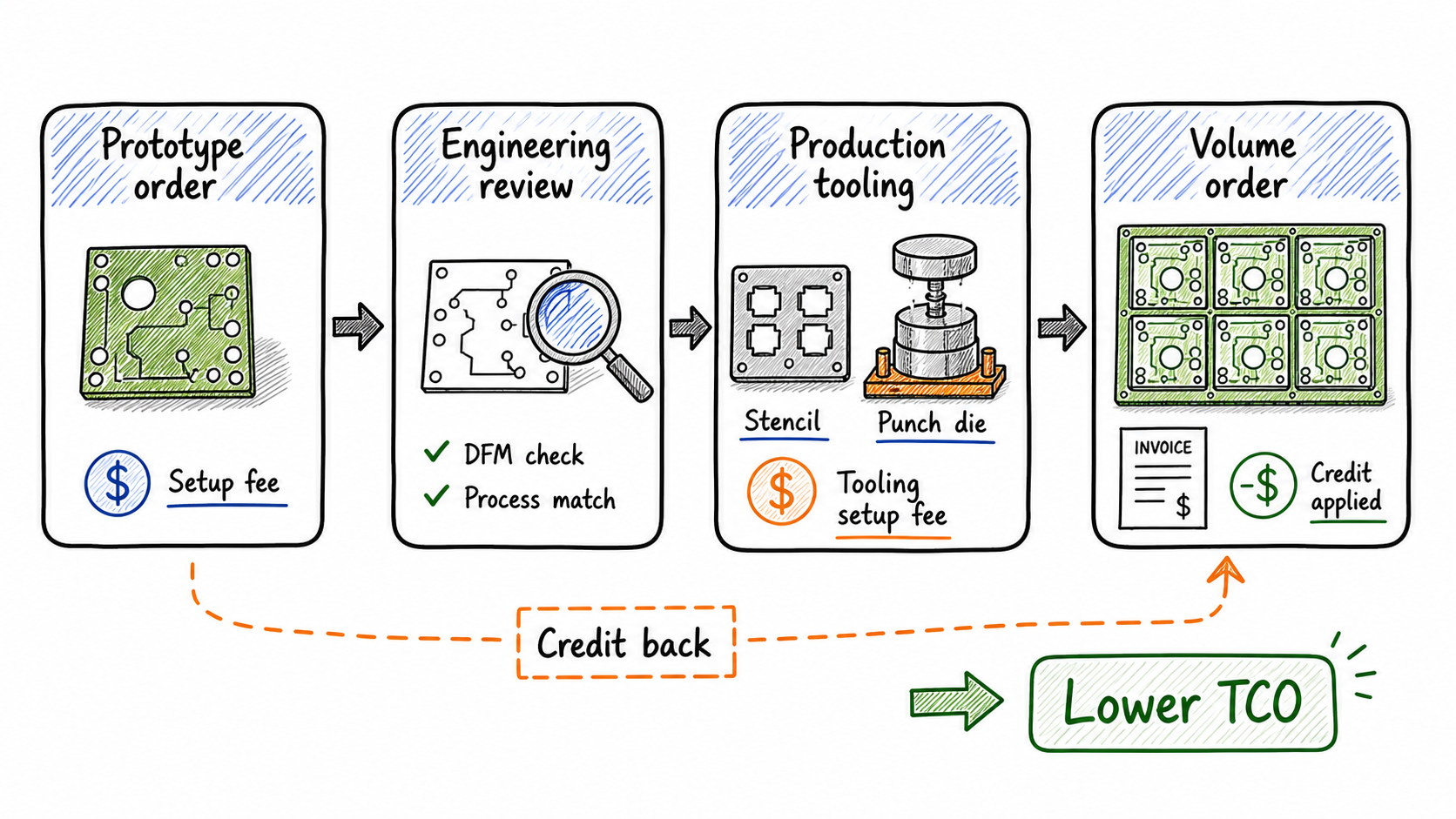 Keeping prototype and volume production with the same factory can reduce duplicated tooling work and allow setup fees to be credited into the production order.
This offsets your early R&D costs while maintaining process and material consistency.
A Practical DFM Checklist for Your First LED PCB Prototype
Before you export your Gerber files and request a quote, verify these parameters to ensure your prototype can scale:
- Substrate Specification: Clearly define your board thickness, typically 1.6 mm, and dielectric thermal conductivity, often 1.0 to 1.5 W/mK, on your drawing.
- Copper Weight: Confirm if 1 oz (35 um) is necessary, or if 0.5 oz (18 um) is sufficient to reduce material costs.
- Edge Keep-Out: Keep all active copper traces at least 0.5 mm away from the profile edge to allow for V-scoring or punch die stamping.
- Drill Files: Include complete NC drill files, even if the design only has non-plated mounting holes.
- Silkscreen Markings: Add clear polarity markings for high-power LEDs to prevent placement errors on automated SMT lines.
Conclusion
Prototyping an LED aluminum board is about validating a manufacturing system that can scale without quality failures or cost shocks.
Chasing low-cost prototypes without considering raw material consistency and mass-production cutting methods can lead to expensive redesigns later.
If you are choosing specifications for an LED aluminum PCB project, send us your drawing, board thickness, copper thickness, surface finish, and target order quantity.
Our engineering team will review your parameters and provide a unified quote for both prototyping and mass production.
Need a quotation?
Send Gerber files and basic specifications. We reply within 1 business day.
Ask for Quote