PCB Files for Manufacturing: What to Send and What to Check

On This Page
PCB Files for Manufacturing: What to Send and What to Check
A PCB file can mean a native design file, a Gerber package, drill data, assembly files, or a full manufacturing exchange format.
For production, don't rely on one .pcb, CAD, or PDF file alone.
A complete handoff includes verified fabrication files, drill files, a fabrication drawing, and — when assembly is needed — BOM and pick-and-place data. A file that looks complete on your end may not be complete enough for quotation, fabrication, SMT assembly, or mass production.
What Is a PCB File?
A PCB file is any digital file used to design, describe, fabricate, assemble, inspect, or test a printed circuit board.
The confusing part is that "PCB file" does not refer to only one format. It can mean the original design file from EDA software, the manufacturing files sent to a factory, or assembly documents like BOM and pick-and-place files.
From a factory point of view, the file extension matters less than the production information inside the package. Here is what each type actually does:
| File Type | Example Format | Main Use |
|---|---|---|
| Native PCB design file | .pcb, .PcbDoc, .brd, .kicad_pcb | Editing and design review |
| Gerber files | .gbr, .gtl, .gbl, .gts, .gbo | PCB layer data for fabrication |
| NC drill files | .drl, .xln | Hole and drill data |
| Fabrication drawing | PDF, DXF, DWG | Human-readable build notes |
| BOM | .csv, .xlsx | Component purchasing and assembly |
| Pick-and-place file | .csv, .txt | SMT placement position and rotation |
| ODB++ / IPC-2581 | Structured manufacturing package | Richer production data exchange |
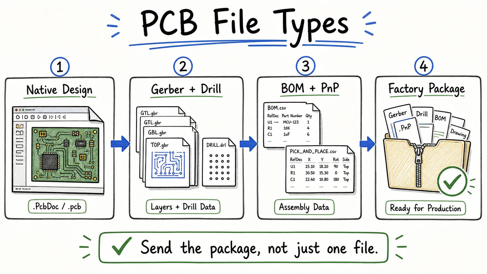 A production handoff usually combines design reference, fabrication data, drill files, and assembly data.
Ucamco describes Gerber as a standard format for PCB design data transfer — which is why it is still the most common format you send to board factories. But Gerber is only one part of the handoff.
The real question is: can the factory quote, build, inspect, and assemble the board without guessing?
Native PCB Files Are Not the Same as Manufacturing Files
Native PCB files are useful for editing and review. Manufacturing files are what the factory needs to actually build the board.
A factory usually needs exported production data, not just the original design file. A .PcbDoc, .brd, or .kicad_pcb file may contain the full design — but it is still tied to the EDA software that created it. Version differences, missing libraries, and unclear export options can change how the file looks on the other side.
Manufacturing outputs are different. They are exported specifically for CAM, drilling, routing, solder mask, silkscreen, assembly, inspection, and test.
Altium's manufacturing documentation separates design work from manufacturing outputs for this reason. The editable design file is not the same as the production release package.
When you're not sure what to send:
- include the native file as a reference if it's available
- send Gerber or supported manufacturing data for production
- include drill files
- include a fabrication drawing
- include assembly files if SMT is required
That removes the guesswork on both sides.
Why Sending Only One .pcb File Can Be Risky
In one Lumina project, a customer sent a native .pcb file. The design looked finished on their end. When the factory opened it, two pads were missing.
The issue did not reach production that time. But it exposed something worth understanding: the file the customer believed they sent was not exactly the file the factory saw after opening it.
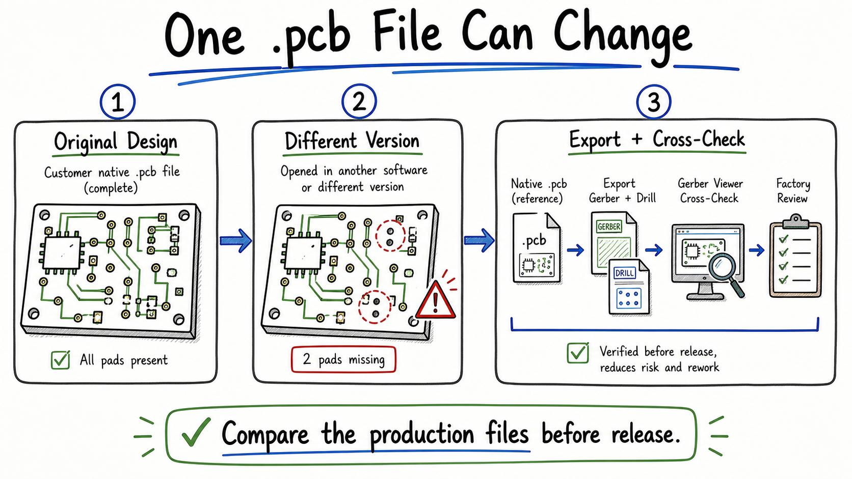 A native PCB file can display differently after version conversion or import, so production outputs should be cross-checked before release.
Native files are tied to the EDA software that created them. Version differences, missing libraries, different layer settings, or unclear export options can change how a file looks on the other side. In some projects, the difference is only found during CAM review.
For a sample order, that delay lands on your schedule. For a repeat LED board, it can create confusion between revisions at exactly the wrong time.
Send the native .pcb file as a backup reference if you want — but send the actual production package separately: exported fabrication files, drill files, drawings, and assembly data if needed.
Before sending, open the exported files in a Gerber viewer and compare them against the design. This catches missing pads, outline errors, and drill alignment problems before the file reaches the factory.
What Files Are Needed for PCB Fabrication?
For PCB fabrication, send Gerber files, drill data, a board outline, and a fabrication drawing with your build requirements.
Gerber files alone are enough for a first review — but not for production. The factory also needs hole data, mechanical details, surface finish, thickness, and special notes.
| File / Note | What It Tells the Factory | When It Is Needed |
|---|---|---|
| Gerber layers | Copper, solder mask, silkscreen, paste, and other layer images | Almost every fabrication order |
| NC drill file | Hole sizes and locations | Boards with holes, vias, slots, or mounting holes |
| Rout / profile data | Board outline, slots, cutouts, panel profile | Non-rectangular boards or panelized boards |
| Fabrication drawing | Thickness, stackup, finish, tolerances, notes | Production release, special requirements |
| Netlist / test notes | Electrical checking reference | When requested or for more controlled builds |
Gerber is common because nearly every factory can process it. But Gerber describes layer images, not build specs — which is why the fabrication drawing still matters.
For LED aluminum PCB fabrication, your drawing or order notes should also confirm board thickness, copper thickness, surface finish, solder mask, and any special mechanical requirements. If the project is for aluminum PCB fabrication, don't send copper artwork alone and assume the factory will infer the rest.
Quotation may start with partial files. Production should not.
What Files Are Needed for PCB Assembly?
If you're ordering assembly, Gerber files alone are not enough. The assembler also needs component and placement data — especially for turnkey SMT assembly.
Gerbers show the board. They don't tell the assembler which LED, resistor, connector, or IC goes on each reference designator.
For bare PCB fabrication: send Gerber, drill, outline, and fabrication drawing. The most common missing item is the drill file or a clear surface finish note.
For SMT assembly: also include BOM, pick-and-place file, assembly drawing, and polarity notes. Rotation and polarity are the most common points that need clarification.
For turnkey PCBA: combine both sets and add sourcing notes — including approved alternates or exact MPNs if substitution is not allowed.
If testing or inspection is part of the project, include test point references and acceptance criteria.
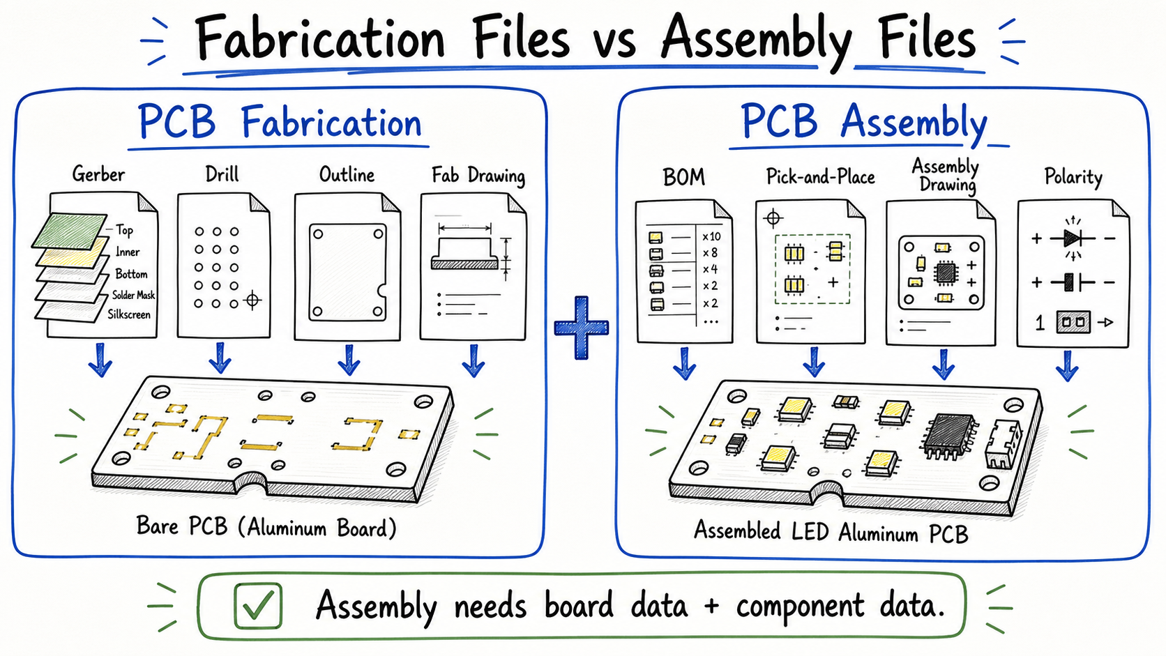 PCB assembly needs the fabrication package plus component, placement, polarity, and sourcing data.
Your BOM should include reference designators, quantities, part numbers, and approved alternatives. Your pick-and-place file should include X/Y position, rotation, side, and reference designator.
Altium's assembly output documentation covers pick-and-place output formats in detail.
For LED boards, polarity deserves extra attention. LED direction, diode polarity, IC pin 1, electrolytic capacitors, and connector orientation should be clear in the assembly drawing or notes.
If assembly is part of the order, link the file package to your SMT assembly for LED aluminum PCB requirements. For a full sourcing and placement project, the same applies to turnkey PCB assembly.
Gerber, Drill, ODB++, and IPC-2581 in Plain Terms
Gerber and NC drill files are the most widely accepted baseline — nearly every factory can process them. ODB++ and IPC-2581 carry richer manufacturing data, but the right choice depends on what your factory can actually handle.
Gerber describes each layer as an image. It is easy to inspect with a viewer and universally supported, but it needs drill files and a fabrication drawing to carry the full build intent.
NC drill files define hole coordinates and sizes. They are not optional — without them, the factory cannot drill your board.
ODB++ and IPC-2581 bundle fabrication, assembly, and test data into a single structured package. When the factory supports them, they reduce back-and-forth. When the factory does not, they create confusion.
Use the format your factory confirms, and include drawings or notes when the format does not carry enough production intent. A rich format is only useful if both sides can open and read it the same way.
Are CAD Drawings or PDFs Enough for PCB Production?
No — but they are still worth including.
Some customers send a DWG drawing and assume the factory will build the board from it. A drawing can describe a shape and list dimensions. It cannot replace Gerber layer data, drill files, BOM, or pick-and-place data — the machine-readable formats that drive fabrication and assembly.
A fabrication drawing PDF can carry board thickness, tolerances, surface finish, and special notes that Gerber files alone do not. An assembly drawing PDF can clarify polarity and placement intent. Both support the file package. Neither replaces it.
If you only have CAD drawings, the design still needs to be exported into proper PCB manufacturing data before production can start.
Extra File Details for LED Aluminum PCB Orders
If you're ordering an LED aluminum PCB or MCPCB, your file package needs more than copper artwork.
The aluminum base, dielectric layer, copper thickness, surface finish, and assembly requirements all affect the final product — and most of these are not captured in the Gerber files themselves.
| Detail | Why It Matters |
|---|---|
| Finished board thickness | Affects structure fit and mechanical support |
| Copper thickness | Affects current capacity and cost |
| Aluminum base thickness | Affects strength and heat spreading |
| Dielectric thermal conductivity | Affects heat transfer from circuit to aluminum |
| Dielectric thickness | Affects insulation and thermal path |
| Surface finish | Affects solderability and storage life |
| Solder mask / silkscreen | Affects appearance, marking, and assembly clarity |
| Quantity and lead time | Affects material planning and production schedule |
If you're ordering LED lighting boards from Lumina, these details should be reviewed together with the aluminum PCB dielectric and repeat-order requirements. A standard board covered in our aluminum PCB guide may look simple from the Gerber file — but your quote can still be delayed if thickness, copper, surface finish, quantity, or thermal requirement are unclear.
For assembly orders, also include:
- LED BOM
- pick-and-place file
- polarity notes
- assembly drawing
- test requirements if needed
The same Gerber package can lead to different quotes if the material and process details are not specified.
What to Check Before Sending PCB Files to a Factory
Before you send, confirm that your exported manufacturing data matches the design intent and that all files belong to the same revision. A file review takes minutes; a production delay does not.
| Check Item | Why It Matters | Common Issue |
|---|---|---|
| Board outline | Defines final shape and routing | Missing or wrong mechanical layer |
| Drill file | Controls holes and vias | Drill file not exported or wrong units |
| Layer alignment | Prevents copper, mask, and drill mismatch | Mirrored or shifted layer |
| Solder mask | Affects soldering and exposed copper | Missing mask opening or wrong side |
| Silkscreen | Helps assembly and marking | Text over pads or missing polarity mark |
| Pads and footprints | Affects soldering and placement | Missing pads after file import |
| BOM revision | Controls component sourcing | BOM does not match Gerber revision |
| Pick-and-place | Controls SMT placement | Rotation or side not clear |
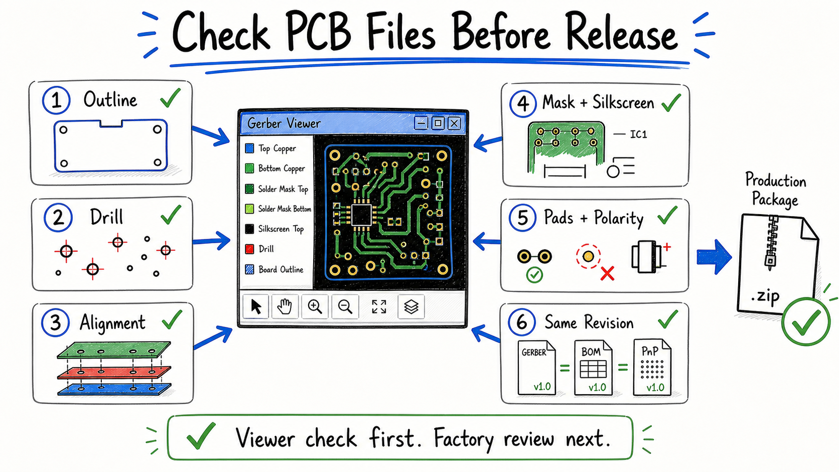 Check the exported package in a viewer, then confirm that the Gerber, drill, BOM, and placement files use the same revision.
Open the exported Gerber or supported manufacturing package in a viewer. Check the board outline, drill holes, slots, solder mask, silkscreen, missing pads, units, scale, and polarity. Then compare the output against the source design or PDF drawing.
If assembly is required, confirm your BOM and pick-and-place file match the same revision as the Gerbers.
For a new LED aluminum PCB project, include a short readme or drawing note listing board thickness, copper thickness, surface finish, quantity, lead time, and any special assembly requirements.
Small checks before quotation often prevent bigger discussions after production has started.
Conclusion
A PCB file is not always a production-ready file.
The most common mistake is not a wrong format — it is an incomplete package. You send Gerbers, assume the factory has everything, and the question comes back days later: drill data is missing, surface finish is unclear, or the BOM does not match the revision.
Think in terms of a handoff, not a file. Fabrication files, drill data, a drawing, and assembly documents if SMT is involved. For LED aluminum PCB, add the thermal and build specs.
If you are not sure whether your file package is complete, send it to Lumina before quoting. We can review the package and identify what may still need confirmation.
Join Our Industrial Community
Get exclusive technical whitepapers and industry news delivered to your inbox every month. No spam, only professional insights.