ENIG on Aluminum PCB: When LED Projects Actually Need It

On This Page (Table of Contents)
Yes, ENIG can be used on an aluminum PCB. Whether it is worth specifying depends on how the board will be assembled, stored, and used.
On a single-sided LED aluminum PCB, ENIG is applied to the exposed copper pads. The aluminum base still provides the thermal and mechanical support. ENIG does not coat that base or improve the board's heat dissipation.
Choose ENIG mainly for flatter pads and better solderability after storage. It can also help when SMT pads are small or closely spaced. For simple, cost-sensitive LED boards, LF-HASL or OSP is often enough.
If you are comparing several finishes, our aluminum PCB surface finish guide provides a broader overview. This article focuses on when ENIG makes sense for LED aluminum boards.
What ENIG Means on an Aluminum PCB
ENIG stands for electroless nickel immersion gold. It consists of an electroless nickel layer covered by a very thin layer of immersion gold.
The finish is applied to exposed copper features, mainly the component pads. During soldering, the gold dissolves into the solder. The nickel remains as the barrier layer and soldering interface. The aluminum base is not part of this process.
Changing from OSP or LF-HASL to ENIG does not change the basic IMS structure. It only changes the finish on the exposed copper.
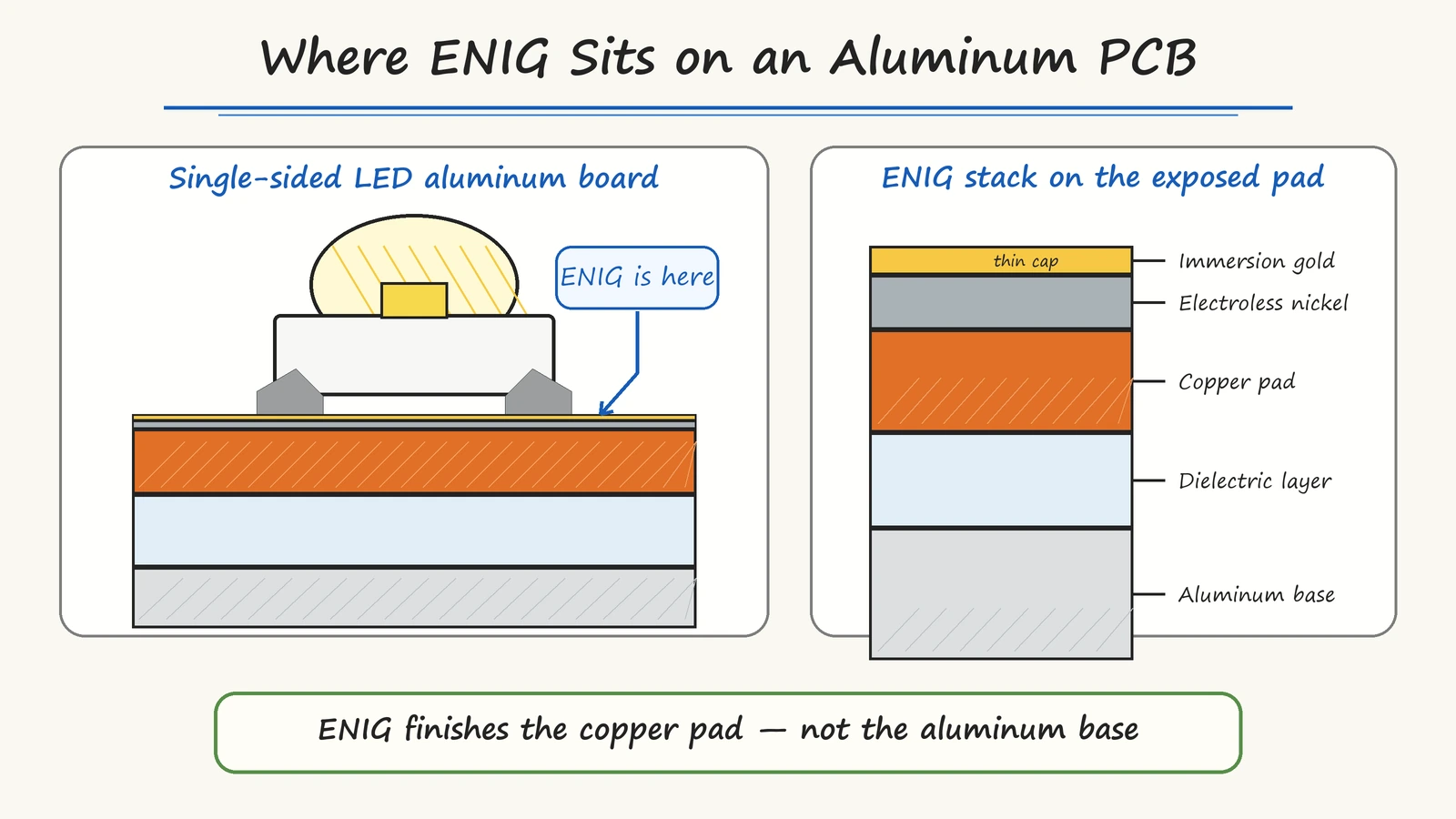
| Layer | Role on an LED aluminum board |
|---|---|
| Immersion gold | Protects the nickel from oxidation before assembly |
| Electroless nickel | Provides the barrier layer beneath the gold |
| Copper pad | Forms the circuit surface to be soldered |
| Dielectric and aluminum base | Provide electrical insulation, heat transfer, and mechanical support |
ENIG thickness is normally controlled through the applicable fabrication specification. IPC-4552 is the main performance framework for ENIG on printed boards. It covers thickness, solderability, and process risks such as hyper-corrosion. Exact requirements depend on the specification revision and the fabricator's process.
A drawing should therefore state ENIG clearly. Avoid a vague note such as “gold finish.” Würth Elektronik's IMS design rules list ENIG as a copper-side finish for metal-core boards. The same document also lists HASL, LF-HASL, OSP, and immersion silver.
The practical point is simple: ENIG changes the solderable copper surface. It does not change the aluminum substrate.
Benefits That Matter for LED Assembly
For LED aluminum boards, the value of ENIG is mainly related to assembly and storage.
Its first advantage is planarity. ENIG is flatter than HASL. This can help with paste printing and component placement. The difference matters more with small pads, fine-pitch parts, or mixed LED and driver packages.
ENIG is also more forgiving when bare boards must be stored before SMT. OSP can work well when boards are handled carefully and assembled soon after production. However, it is more sensitive to storage conditions and repeated handling. Under controlled storage, ENIG usually retains solderability for longer.
A flat, stable finish can give the assembly process more tolerance on a dense layout. However, ENIG cannot correct other process problems. Stencil design, paste printing, placement, and reflow still need proper control.
If PCB fabrication and assembly are being reviewed together, see our SMT assembly for LED aluminum PCB page.
When ENIG Is Worth It—and When It Is Over-Specified
ENIG is worth considering when its flatness or storage advantage solves a real production problem. It is less useful on a simple board with large pads. This is especially true when assembly follows soon after fabrication.
ENIG is usually worth discussing when:
- the board includes small pads or fine-pitch components
- bare boards may remain in storage before SMT assembly
- the layout requires a consistently flat soldering surface
- several package types share the same board and placement tolerance is limited
ENIG may be unnecessary when:
- the board is a simple lighting module with relatively large pads
- assembly follows shortly after PCB production
- LF-HASL topography does not affect the component layout
- OSP storage and handling requirements can be controlled
- ENIG was selected only because it was assumed to be the higher-quality option
| Production situation | Is ENIG usually justified? |
|---|---|
| Fine-pitch components or small pads | Often yes |
| Longer storage before SMT | Often yes |
| Simple volume LED board assembled soon after fabrication | Often no |
| Attempting to improve heat dissipation | No |
Before specifying ENIG, ask what problem the finish is expected to solve. If the answer is pad flatness, storage, or a sensitive SMT layout, the added cost may be justified. If none of those conditions applies, LF-HASL or OSP may be the more practical choice for volume production.
ENIG vs HASL vs OSP for Lighting Buyers
For many LED lighting boards, the initial comparison is between LF-HASL, OSP, and ENIG. The right choice depends more on assembly conditions than on which finish appears more premium.
| Finish | Common fit | Main point to check |
|---|---|---|
| LF-HASL | Cost-sensitive boards with moderate component pitch | Surface is less flat |
| OSP | Flat pads with quick, well-controlled assembly | More sensitive to storage and handling |
| ENIG | Small pads, longer storage, or a less forgiving SMT layout | Higher cost may not add value on a simple board |
LF-HASL offers good solderability at a lower cost, but its surface is less flat. OSP is flat and cost-effective. It works best when storage, handling, and assembly stay within a suitable process window. ENIG offers both flatness and better storage tolerance. Choose it when the project needs both.
For a complete comparison, read the aluminum PCB surface finish guide. The article OSP vs HASL for aluminum PCB covers the two common cost-oriented options. For storage details, see OSP PCB shelf life for LED boards.
Does ENIG Improve Aluminum PCB Heat Dissipation?
ENIG does not meaningfully improve the overall thermal performance of an aluminum PCB.
Heat from an LED normally travels through the following path:
LED → copper circuit → dielectric layer → aluminum base → housing or heatsink
The nickel and gold layers are only micrometers thick. They also sit only on the exposed copper pads. The dielectric, copper geometry, aluminum base, and mounting interface have far more influence on thermal resistance.
If an LED board is running too hot, the more useful areas to review are:
- dielectric thermal conductivity and thickness
- copper thickness, copper area, and circuit layout
- aluminum base construction
- contact between the board and the housing or heatsink
- thermal interface material and mounting pressure
Surface finish should be selected for solderability, planarity, storage, and assembly compatibility. Thermal decisions should be made from the full board and housing structure. Our guide to LED aluminum PCB heat dissipation explains this heat path in more detail.
Why Wire-Bonding ENIG Content May Not Apply to LED SMT Boards
Search results about ENIG often include wire bonding and semiconductor packaging. The information may be correct, but the assembly process is different from standard soldered LED SMT.
Most conventional LED aluminum boards use packaged LEDs and other components assembled with solder paste and reflow. For these boards, the surface finish is chosen mainly for solderability, pad flatness, storage, and process compatibility.
Wire bonding connects a bare die to a pad with a fine metal wire. The result depends on the wire material, bonding method, pad chemistry, and finish thickness. It also requires a qualified bonding process. Some applications need a different or more tightly controlled finish than standard SMT ENIG.
For packaged LEDs and normal reflow, evaluate ENIG as a solderable pad finish. Bare-die or chip-on-board designs need a separate wire-bonding review. Confirm those requirements with a supplier qualified for that process.
What to Confirm Before Production
State the surface finish clearly on the drawing or order notes. “Aluminum PCB” describes the board type, not the finish. The fabricator still needs to know whether the exposed copper requires LF-HASL, OSP, ENIG, or another option.
Before production, confirm:
- the required surface finish on the drawing
- whether the board uses SMT only or another assembly process
- the smallest component package, pad size, or pitch
- the expected time between PCB fabrication and SMT assembly
- storage and packaging conditions for bare boards
- sample or mass-production quantity
- the LED lighting application and any special assembly notes
- the Gerber file, fabrication drawing, or reference sample
If you are deciding between OSP and ENIG, include the component packages with the board files. Also state the expected storage time. These details are more useful than the finish name alone.
For general production scope, see aluminum PCB fabrication for LED lighting.
Conclusion
ENIG makes sense when the board needs flatter pads or better storage tolerance. It can also help with smaller SMT pads. For a simple board assembled soon after fabrication, LF-HASL or OSP may be enough.
Choose the finish around the assembly process. Do not treat it as a general quality upgrade or a substitute for thermal design.
If you are unsure, share the drawing, component details, storage time, and order quantity. We can review the finish together with the rest of the aluminum PCB specification before quotation.
Need a quotation?
Send Gerber files and basic specifications. We reply within 1 business day.
Ask for Quote