Aluminum PCB Routing vs Punching: Real Costs, Burrs, and How to Calculate Break-Even

On This Page (Table of Contents)
Should you route your aluminum PCBs or punch them with a dedicated die?
Route for prototypes and short runs. Punch for volume production.
The real question is when to make the switch.
Many engineering blogs quote a generic crossover between 5,000 and 30,000 pieces. On a real PCB shop floor, piece count is the wrong metric.
A large ceiling panel reaches hundreds of square meters in under 2,000 boards. A tiny spotlight module takes 50,000 boards to cover the same area.
Aluminum PCB factories price volume fabrication by square meters (), not by pieces. You can find your crossover point with one simple formula.
How does that play out on the shop floor?
- Simple linear strips (no holes). Straight routing or V-scoring is fast. CNC routing and die punching often cost nearly the same per square meter.
- Multi-hole boards (downlights, high bays). Rotating bits cut metal-ceramic composites slowly and wear out fast. At our factory (Lumina), CNC routing these boards costs about 10 RMB/m² (~420 USD). That puts our shop-floor break-even right around 300 m²—and we refund the die fee 100% once cumulative orders reach 30X the tooling value.
Unit cost is only half the story.
Die punching also creates downward burrs that can ruin heat sink contact, and inadequate copper pullback can trigger dielectric Hi-Pot flashover or direct electrical shorts.
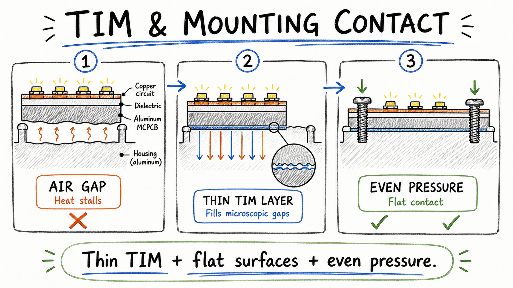 Figure 1: Downward shear burrs act as standoffs, creating air gaps that trap heat under high-power LEDs.
1. Why Aluminum Destroys CNC Bits but Yields to Punch Dies
Cutting an aluminum PCB is a clash between two opposing materials.
Standard FR-4 fiberglass cuts quickly on CNC routing tables. Aluminum substrates do not.
When a rotating bit cuts an aluminum PCB, it fights two wear mechanisms at the same time.
- Soft aluminum sticks to the flutes. Alloys like 5052 and 1060 are ductile. Under cutting friction, hot aluminum welds onto the carbide blade. This Built-Up Edge (BUE) clogs the flutes and snaps small routing bits.
- Hard ceramic grinds the cutting edge. The dielectric insulation layer is packed with aluminum oxide filler (Mohs hardness 9). Those ceramic particles act like sandpaper and wear the bit flat.
One layer welds to the tool. The next layer grinds it down.
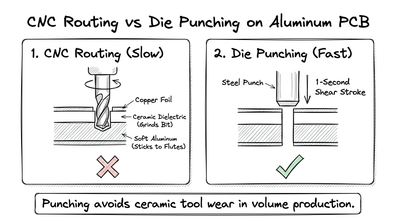 Figure 2: CNC routing bits suffer from ceramic abrasive wear and sticky aluminum chips, while a compound punch die shears the board in one second.
Carbide bits lose their sharp edge within dozens of meters.
To keep bits from snapping, operators have to slow the spindle feed rate way down. Slow feed rates mean high machine-hour costs.
Compound punch dies bypass rotary cutting entirely.
A press does not make chips. Hardened tool steel stamps through the board in a 1-second stroke, separating the part through clean shear fracture under DIN 9830.
Outlines, mounting holes, and lens slots are cut in a single hit. In volume production, a punch press outpaces a CNC router by dozens of times.
| Process Metric | CNC Routing (Milling) | Compound Die Punching | Impact on Luminaire Assembly |
|---|---|---|---|
| Separation Method | Multi-pass rotary cutting | Single-stroke shear fracture | Routing cuts clean paths; punching shears the full outline in one hit |
| Cycle Speed | 2–4 minutes per panel | 1–2 seconds per stroke | Punch presses run dozens of times faster in mass production |
| Tool Wear | High cutter wear from ceramic fill | Low wear on hardened tool steel | Routing drives up machine costs; dies run 50,000+ hits between sharpening |
| Outline Repeatability | Punched boards fit extruded fixtures with tighter consistency | ||
| Edge Defects & Burrs | Break-away tab nubs () and galling lips (heavily dependent on manual hand-deburring) | Continuous vertical exit micro-burrs (, fully automated via brush deburring) | Routing tab nubs cause fixture tilt; unbrushed punch burrs ruin flat heat sink contact |
| Copper Pullback Margin | for low-voltage; for high-voltage / Hi-pot | Punching needs clean edge margin to prevent copper drag and dielectric edge flashover | |
| Initial Tooling NRE | $0 tooling fee | 800 industry range (~¥3,000 / ~$420 at Lumina) | Routing saves upfront cash; punching lowers square-meter prices |
| Volume Break-Even | Lower total cost on small runs | Lower total cost once m² savings cover die fee | ~300 m² typical benchmark at Lumina for multi-hole LED boards |
2. Edge Defects and Thermal Contact: Punch Burrs vs Routing Flashing
On outline tolerance alone, compound punch dies outperform CNC routers.
Slow-wire EDM punch tooling holds outlines within . CNC routing typically drifts between and due to cutter wear and spindle deflection.
If your round downlight board press-fits into an extruded aluminum housing, punched boards drop in with much better consistency.
However, neither process produces a perfectly pristine edge right off the machine. Prototyping platforms often praise CNC routing as "clean and smooth" while blaming all burrs on punching. That ignores the physical reality of the factory floor.
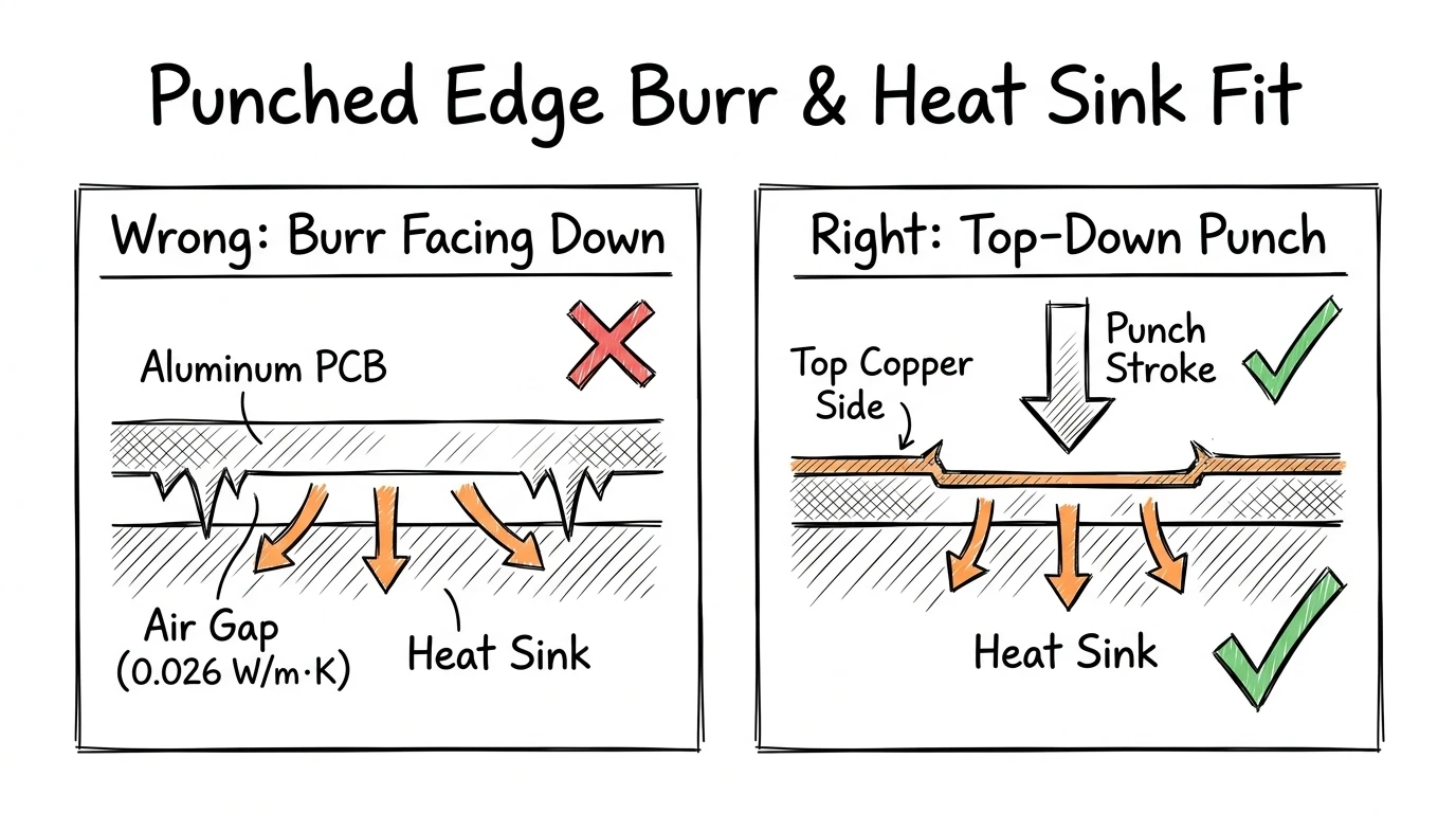 Figure 3: Edge defect comparison: Unbrushed downward punch burrs lift boards off heat sinks, while CNC routing tab nubs and galling lips create mechanical tilt and assembly interference.
Truth 1: Downward Punch Burrs Are a Real Physical Shear Artifact
During the final stage of stamping, metal fractures under tensile shear stress. Under standard shear-fracture mechanics (DIN 9830), the exit burr always forms on the tool exit side—which is the bare aluminum heat sink face.
Standard compound dies use locating pins and poka-yoke tooling that strictly enter from the top copper side down (protecting traces and preventing dielectric delamination). That means: every punched aluminum board naturally comes off the press with downward micro-burrs measuring 5% to 10% of board thickness ( to ).
If a fabricator skips secondary deburring and packs boards straight off the press, serious thermal trouble follows:
- Those continuous micro-burrs act like tiny metal standoffs, lifting the aluminum base right off your fixture housing;
- Static air is a terrible heat conductor (). Even a 0.1 mm micro-gap chokes heat dissipation;
- Thin thermal phase-change films or 100 µm thermal tapes get punctured by the sharp metal edge, driving up LED junction temperatures and triggering rapid lumen decay.
Standard inspection will not protect you here. Under IPC-A-600G (Section 2.1.1), edge burrs are acceptable on Class 1 and Class 2 boards as long as they remain firmly attached and fit within dimensional tolerances.
Truth 2: CNC Routing Is Far from Pristine—Its Defects Are Irregular and Hidden
Many engineers assume routing guarantees a clean board edge, only to fight assembly issues on the production line:
- Break-away tab and mouse-bite protrusions ():
- Routed panels cannot be milled completely free in mid-air. They rely on break-away tabs or perforated mouse bites to stay anchored to the panel frame.
- After tab breaking or nipping, jagged aluminum nubs protrude from the outline. If these nubs land near a housing alignment rail, they cock the board at an angle or scratch the fixture.
- Adhesive galling lips and bottom flashing from tool wear:
- Abrasive ceramic particles inside the dielectric dull carbide router bits quickly. Once a cutter loses its sharp edge, it stops cleanly shearing ductile 5052 aluminum and starts smearing it under frictional heat.
- This rolls a stubborn, irregular aluminum lip (flashing) along the bottom edge that compressed air blowers cannot remove.
- Lead-in marks and internal corner radius limits:
- Spindle plunge points leave small step marks, and rotary cutters cannot mill sharp internal corners (leaving an inside radius of ), creating mechanical interference against square chassis pockets.
The Real Difference: Automated Deburring vs Error-Prone Hand Scraping
Since both processes generate edge artifacts, why do high-volume lighting factories still favor compound punching?
Because the remediation cost and consistency are completely different:
- Punched burrs are uniform and continuous.
A quality factory runs stamped boards through an automated double-sided brush deburring machine or vibratory finishing tumbler. Conveyor rollers pass panels through abrasive nylon wheel brushes, radius-breaking every perimeter and hole edge to ISO 13715 (
-0.05 mm) in seconds. The process is 100% automated with zero human variance. - Routing nubs and galling lips are localized and irregular. Automated brush rollers cannot grind down protruding break tabs, and stubborn aluminum flashing resists quick buffing. Shops must assign operators to scrape edges by hand with utility knives or deburring blades. If a worker gets tired and misses a tab nub, that board lands on your assembly line and jams your housing.
The professional DFM takeaway is straightforward:
- Call out ISO 13715 edge conditions (
-0.05 mm, no positive burrs or protruding tabs) on your print regardless of the process; - Verify that your volume punch supplier runs automated brush deburring inline.
3. Edge Clearances: Mechanical Anti-Shorting and Dielectric Hi-Pot Rules
In single-layer MCPCB profiling, copper pullback from the edge serves two distinct, non-negotiable engineering requirements:
- Mechanical isolation: Preventing sheared copper burrs and smearing from shorting to the aluminum plate.
- Electrical safety and creepage: Preventing board-edge flashover and dielectric breakdown during high-voltage Hi-Pot testing.
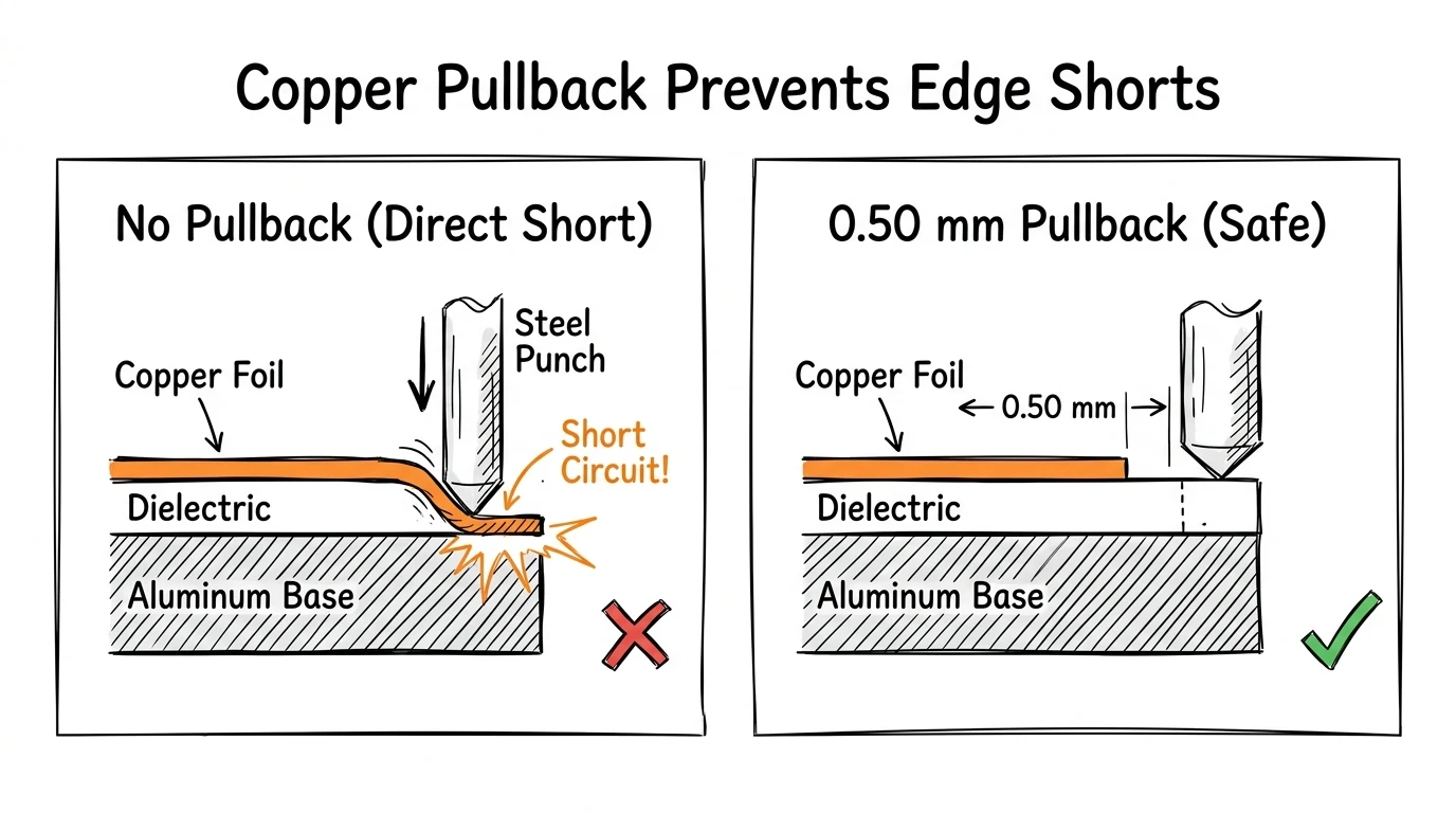 Figure 4: Without sufficient edge clearance, the punch drags ductile copper across the thin dielectric layer into the aluminum base. Adequate pullback blocks both mechanical copper drag and high-voltage surface arcing.
Risk 1: Mechanical Copper Smearing and Dead Shorts
Electrolytic copper foil is highly ductile. When a hardened steel punch shears down through the laminate, intense shear stress pulls the copper downward (known on the shop floor as "copper drag" or smearing).
This drags microscopic copper slivers across the thin () dielectric edge.
If copper traces run right to the board edge, those dragged slivers bridge straight into the raw aluminum baseplate. The result is an immediate 0-ohm dead short or severe leakage current into the metal luminaire fixture.
Risk 2: Board-Edge Hi-Pot Breakdown and Flashover
Many engineers solve mechanical shorts only to watch entire production batches fail Hi-Pot (dielectric withstand) testing on the assembly line.
Inside the board, the core dielectric layer isolates reliably. But the cut edge is an open, vulnerable boundary:
- Shearing and routing exert severe localized mechanical stress that induces micro-cracks and micro-delamination along the exposed dielectric wall, while also attracting airborne conductive dust.
- The dielectric thickness is only (). If copper traces sit right on the edge, the surface creepage distance between live copper and the chassis-grounded aluminum base is severely compromised.
Commercial and industrial LED fixtures regularly require dielectric withstand tests under IEC 60598-1 or UL 8750 (typically 1,500V to 3,000V AC). If edge clearances are too tight, high voltage will not pierce through the cured dielectric core; it will spark and arc over the exposed board edge through the air and across the sheared boundary (surface flashover).
How Much Copper Pullback Do You Actually Need?
Legacy laminate design guides (like older Bergquist manuals) often cited a strict rule: , demanding a 1.50 mm pullback on a 1.0 mm board.
That recommendation was never about "crude tooling from the past." It was formulated specifically to guarantee high-voltage safety creepage and 3 kV Hi-Pot isolation.
In production DFM, choose your edge pullback based on your operating voltage and safety testing criteria:
- Scenario A: Low-voltage isolated / SELV systems (, no Hi-Pot or )
- Mechanical drag is the only constraint.
- As long as the press stamps top-down with sharp dies and solder mask coats the perimeter, a pullback reliably stops copper shorts while saving tight trace space on narrow linear boards.
- Scenario B: Non-isolated drivers / direct AC / high-voltage certification (Hi-Pot )
- Creepage distance and air flashover govern your design.
- Never squeeze pullback down to 0.50 mm. Keep traces at least away from punched edges, and verify that your white solder mask cleanly overlaps the dielectric step.
- Scenario C: Heavy boards ( aluminum base)
- Deeper fracture zones and greater copper deformation require clearance regardless of operating voltage.
What if your optical layout forces solder pads closer than 0.50 mm to the perimeter?
On low-voltage boards, ask your PCB supplier to machine circuit relief cavities into the punch die. Toolmakers mill away die steel above trace zones so punch blades never pinch copper foil. Note that relief cavities only prevent mechanical smearing; they cannot bridge creepage gaps on high-voltage Hi-Pot boards.
Catching these clearances before tooling prevents single-layer MCPCB dielectric breakdown once mass production ramps.
4. How to Calculate Your Break-Even Area (Plus Factory Numbers)
Every PCB factory has slightly different tooling rates and machine hourly costs.
Still, the underlying math is universal. In volume production, factories quote aluminum PCBs per square meter ().
To find when die punching pays for itself at any supplier, divide their upfront die fee by the per-square-meter price gap between routing and punching.
Why does CNC routing cost more per square meter?
A multi-spindle router takes 2 to 4 minutes to trace around boards on a panel, drill mounting holes, and mill cutouts. An automatic punch press stamps the whole panel in 1 to 2 seconds. With routing, you are paying for machine time and worn-out carbide bits.
That also means board geometry changes the math.
- Simple linear boards (no holes). A 1-meter LED strip with zero internal holes can be cut with straight passes or fast V-scoring. On these boards, CNC routing and die punching often cost almost the same per square meter. There is no rush to open a die.
- Multi-hole downlights and high bays. A round board with 4 screw holes, 2 wire slots, and lens notches takes dozens of drill hits and slow circular milling. Here, punching saves serious money.
Real Factory Benchmark (How the Math Works at Lumina)
To give you concrete numbers for your spreadsheet, here is how we price single-sided aluminum PCBs at our factory (Lumina).
- CNC routing vs. punching price gap. For typical multi-hole boards, CNC routing costs about 10 RMB/m² (~$1.4/m²) more than die punching.
- Dedicated compound die fee. Around ¥3,000 (~$420 USD).
Plug those numbers into the formula.
At our factory, 300 m² is the standard crossover point.
Under 300 m², stick with CNC routing and keep your cash. Past 300 m², the ¥10/m² processing savings have fully paid for the die, and every square meter after that lowers your unit cost.
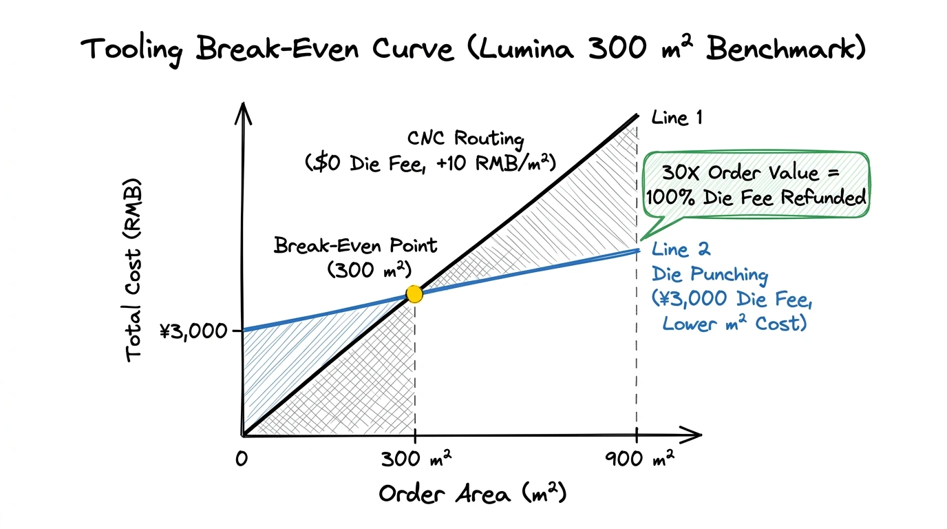 Figure 5: At our factory benchmark (¥3,000 die fee and ¥10/m² routing gap), die punching breaks even at 300 m² and qualifies for a 100% die refund at 30X order value.
How Tooling Refunds Work (Our 30X Policy)
Buyers often hesitate to pay upfront tooling fees because they worry a product revision will turn the die into scrap metal.
When you quote volume orders, always ask your supplier if they offer a tooling rebate.
At Lumina, we use a straightforward 30X tooling refund policy.
Once your cumulative production orders for that board reach 30 times the tooling fee (about ¥90,000 / ~$12,600 USD, or roughly 800 to 1,000 m² of boards), we refund the initial ¥3,000 die fee in full on your invoice.
You keep ownership of the die, and our shop covers routine sharpening and maintenance for repeat orders.
This machine-hour math also explains why unit prices plateau on fast-turn sites like JLCPCB or PCBWay. Those platforms are built for fast-turn PCB prototyping through shared CNC panels, not dedicated press tooling. You can compare more of these volume drivers in our breakdown of aluminum PCB manufacturing cost factors.
5. Quick Decision Checklist: Route or Punch?
Use this checklist to match your separation method to your order stage and board design.
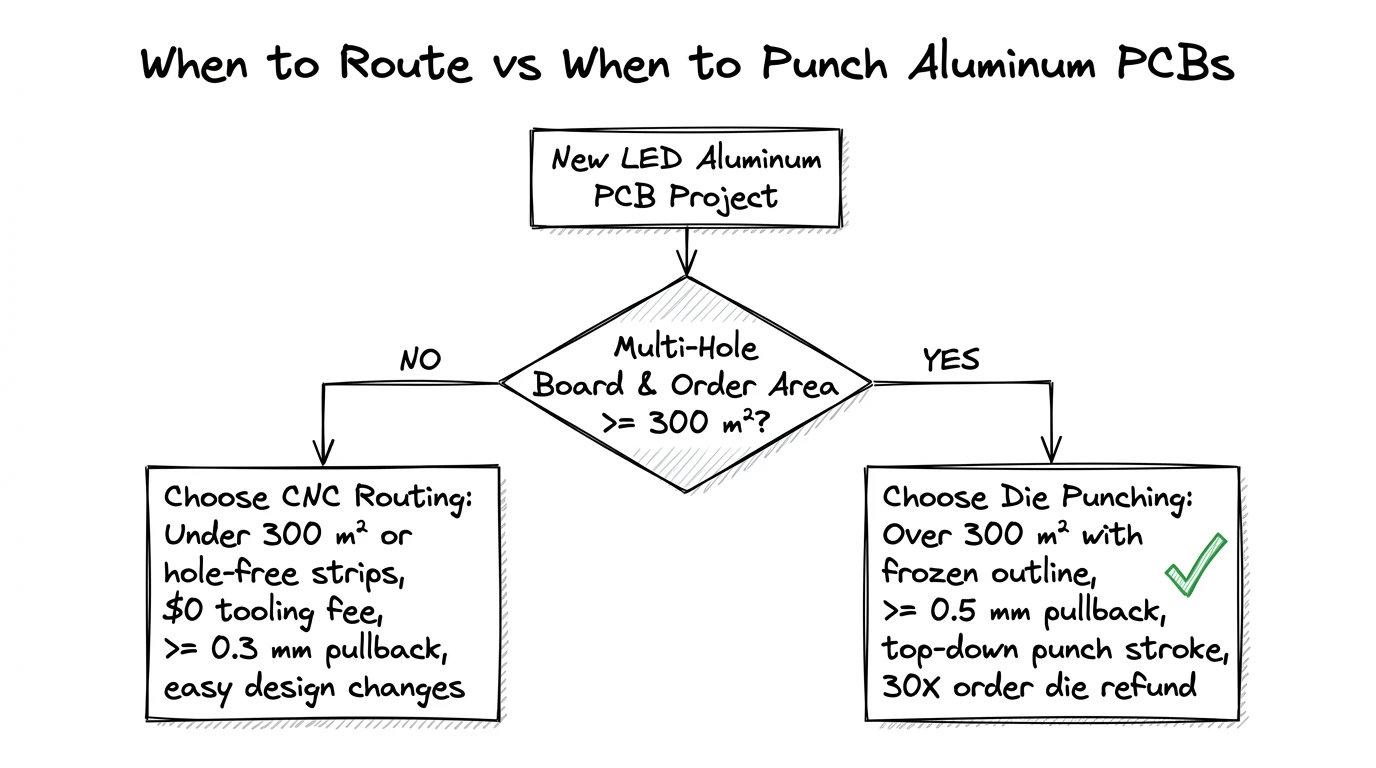 Figure 6: Route prototypes and hole-free linear strips; switch to compound die punching once multi-hole boards pass the ~300 m² break-even point.
Stick with CNC routing when
- Your total order area is below break-even (under ~300 m² for typical multi-hole boards).
- Housing dimensions, screw holes, or lens cutouts might still change.
- Your board is a simple, hole-free linear strip where routing and V-scoring carry no price penalty.
- You need fast prototypes right away without waiting a few days to build a die.
Switch to compound die punching when
- Your single order or scheduled repeat volume passes the break-even mark (~300 m²).
- Mechanical dimensions and hole positions are 100% frozen.
- The board has several mounting holes, wire slots, or round contours that slow down CNC spindles.
- Your housing assembly needs tight outline repeatability.
- Your cumulative volume will hit the supplier's rebate mark (such as our 30X order refund).
4 Gerber checks before you cut steel
- Minimum hole diameter. Punch hole diameter must equal or exceed aluminum thickness (). Trying to punch a 0.8 mm hole through a 1.5 mm aluminum board will snap the punch pins.
- Hole-to-edge spacing. Keep holes at least away from the board edge so the aluminum web does not warp under press tonnage.
- Copper pullback. Keep traces and pours at least 0.50 mm back from punched edges for low-voltage SELV designs, and increase to 1.0–1.5 mm for non-isolated high-voltage circuits (Hi-pot ) or boards thick.
- Deburring callout. Specify an ISO 13715 edge condition (
-0.05 mm) on your drawing to require post-stamping brush deburring, ensuring a flat heat sink face with zero positive burrs.
Lead times depend on order size, board complexity, and line scheduling. CNC routed samples move fast once raw laminate is staged, while building and proofing a compound punch die takes a few extra working days upfront before high-speed stamping takes over.
Final Takeaway
Don't judge aluminum PCB profiling by piece count or upfront tooling fees alone.
Run the square-meter math for your specific board. Keep hole-free linear strips on CNC routers or V-cut machines, and move multi-hole volume boards to punch dies once your order area crosses break-even (~300 m² at our factory). Size your copper pullback to match your dielectric withstand requirements (0.50 mm for SELV, 1.0–1.5 mm for high-voltage Hi-Pot), ensure your supplier runs post-punch deburring, and your boards will drop into their housings flat, short-free, and insulation-safe.
Need a quotation?
Send Gerber files and basic specifications. We reply within 1 business day.
Ask for Quote